Optical proximity correcting method

An optical proximity correction, photomask technology, applied in optics, originals for optomechanical processing, special data processing applications, etc., to achieve the effect of improving exposure accuracy

Active Publication Date: 2005-03-09
NAN YA TECH
View PDF0 Cites 7 Cited by
  • Summary
  • Abstract
  • Description
  • Claims
  • Application Information

AI Technical Summary

Problems solved by technology

[0019] Therefore the main purpose of the present invention is to provide a kind of optical proximity correction method that first carries out reference type optical p

Method used


Image

  • Optical proximity correcting method
  • Optical proximity correcting method
  • Optical proximity correcting method

Examples


Embodiment Construction

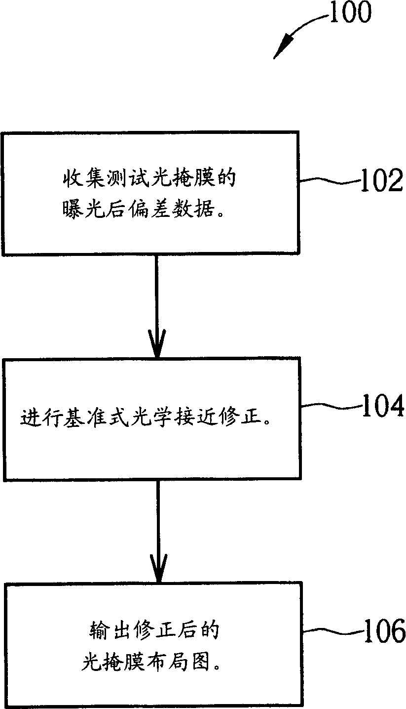
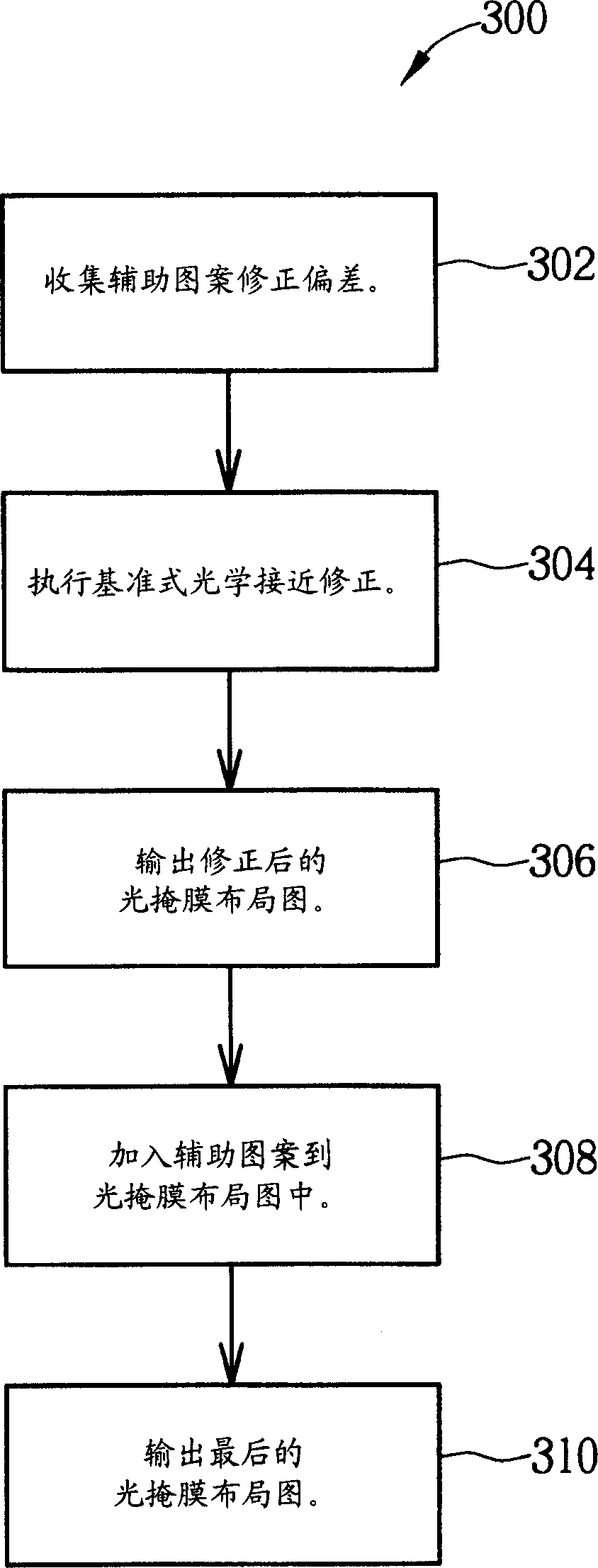
[0027] Please refer to image 3 , image 3 It is a schematic flowchart of a process 300 for modifying a photomask layout by the optical proximity correction method of the present invention, wherein the photomask layout includes at least one photomask pattern. The correction process 300 includes the following steps:

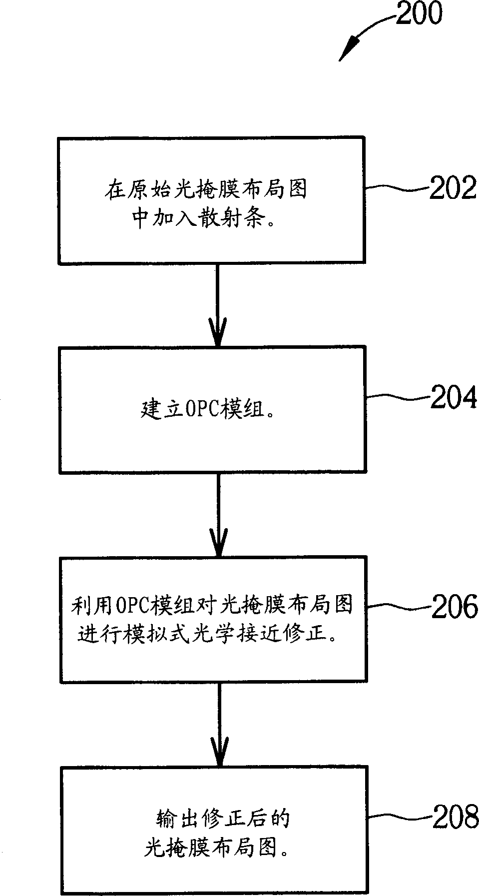
[0028] Step 302: Collect auxiliary pattern correction deviation values ​​of the first auxiliary patterns scheduled to be added to the photomask layout pattern, establish an auxiliary pattern correction model similar to a database, and collect exposure deviation value data of the original photomask pattern at the same time. In this step, the first auxiliary pattern to be added may be a scattering strip. The implementation method of this step can use the test photomask to measure the deviation value of the photomask pattern that needs to be corrected, so as to obtain the proper adding position and size of the scattering strips.

[0029]Step 304: Combining with th...


PUM


Abstract

The present invention provides an optical proximity correction method for photomask placement diagram, in which said photomask diagram at least includes one photomask pattern. Said method includes the following steps: collecting auxiliary pattern correction deviation value of auxiliary pattern which is one of predefined auxiliary patterns to be added into said photomask placement diagram; then combining said auxiliary pattern correction deviation value to make reference type optical proximity correction, calculating target correction deviation value required for correction of said photomask pattern and according to the calculated result make correction of said photomask pattern, outputting corrected photomask placement diagram, finally adding said auxiliary pattern into said corrected photomask placement diagram.

Description

technical field [0001] The present invention relates to an optical proximity correction method (optical proximity correction, OPC), in particular to a standard (rule-based) optical proximity correction, and then adding auxiliary patterns such as scattering bars (scattering bar) after correction Optical proximity correction method for photomask patterns. Background technique [0002] In the semiconductor manufacturing process, in order to smoothly transfer the pattern of integrated circuits (integrated circuits) to the semiconductor chip, the circuit pattern must first be designed on the photomask layout, and then the photomask output according to the photomask layout A photomask pattern is used to make a photomask, and the pattern on the photomask is transferred to the semiconductor chip in a certain proportion. [0003] Since the critical dimension (CD) of the patterns that can be produced on the photomask is limited by the resolution limit of the optical exposure tool, wh...

Claims


Application Information

Patent Timeline
IPC IPC(8): G03F1/36G03F9/00G06F17/50
Inventor 刘淑慧吴文彬
Owner NAN YA TECH
Why Eureka
Try Eureka