Liquid crystal display device and its manufacturing method

A liquid crystal display device, liquid crystal technology, applied in identification devices, semiconductor/solid-state device manufacturing, static indicators, etc.

Inactive Publication Date: 2005-04-06
AU OPTRONICS CORP +1
View PDF3 Cites 2 Cited by
  • Summary
  • Abstract
  • Description
  • Claims
  • Application Information

AI Technical Summary

Problems solved by technology

The variation of the channel length is due to a large change in the ON current value of the insulated gate transistor, so it usually requires strict manufacturing management. However, the length of the channel, that is, the pattern size of the screen exposure area is affected by the exposure amount (light source intensity) and the pattern accuracy of the photomask, especially the line and space dimensions), the coating thickness of the photosensitive resin

Method used


Image

  • Liquid crystal display device and its manufacturing method
  • Liquid crystal display device and its manufacturing method
  • Liquid crystal display device and its manufacturing method

Examples


Embodiment 1

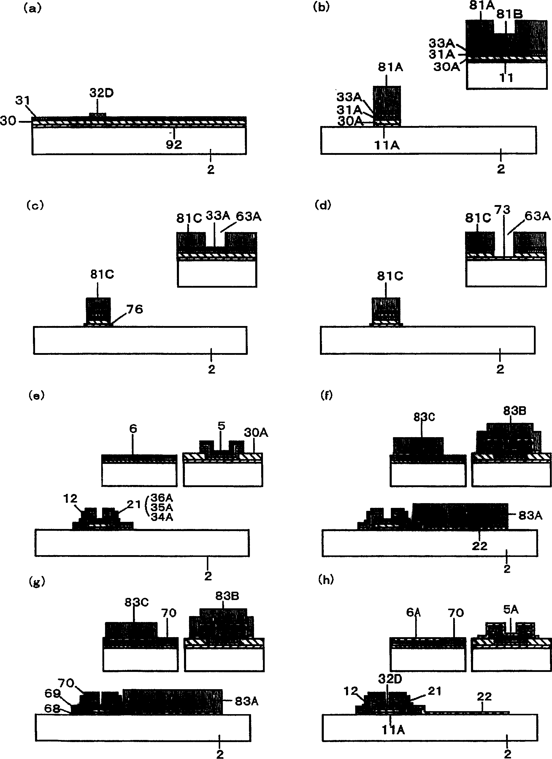
[0111] In Example 1, as in the conventional example, first, on the main surface of the glass substrate 2, use a vacuum film forming device such as SPT to coat, for example, Cr, Ta, Mo, etc. or alloys or silicides of these metals to form a film thickness The first metal layer is about 0.1 to 0.3 μm. In the present invention, in the case of selecting an organic insulating layer as the insulating layer formed on the side of the scanning line, there is almost no limit to the material of the scanning line; but in the case of selecting an anodized layer as the insulating layer formed on the side of the scanning line , It is necessary to keep the anodized layer insulating. In this case, considering the high resistance of Ta alone and the lack of heat resistance of Al alone, the heat resistance can be selected for the low resistance of the scanning line. Higher single-layer structure of Al(Zr, Ta, Nd) alloy or layered structure of Al / Ta, Ta / Al / Ta, Al / Al(Ta, Zr, Nd) alloy as the struct...

Embodiment 2

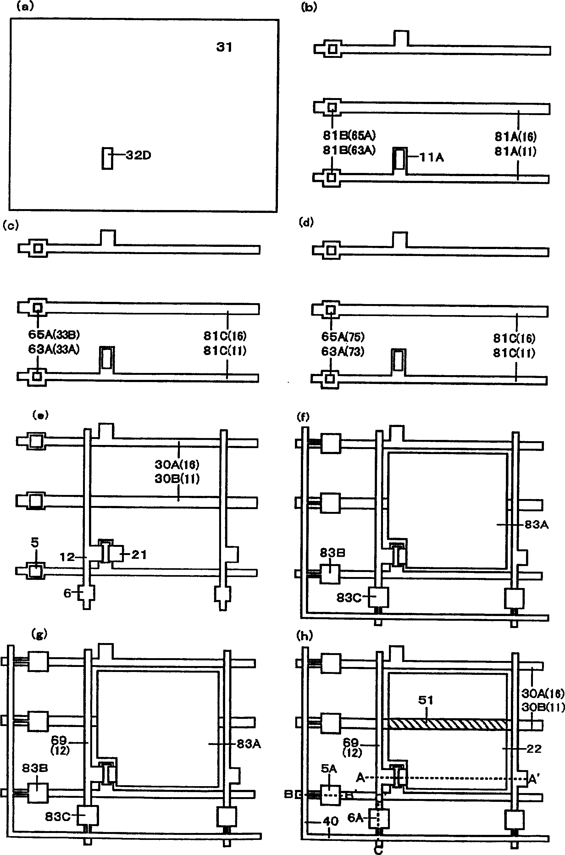
[0127] In Example 2, such as image 3 (d) and Figure 4 As shown in (d), the contact forming process is performed, that is, the second amorphous silicon layer 33A, 33B in the opening 63A, 65A, the first amorphous silicon layer 31A, 31B, and the gate insulating layer are selectively etched. 30A, 30B, and before exposing a part 73 of each scanning line 11 and a part 75 of the storage capacitor line 16, the same manufacturing process as in the first embodiment is performed.

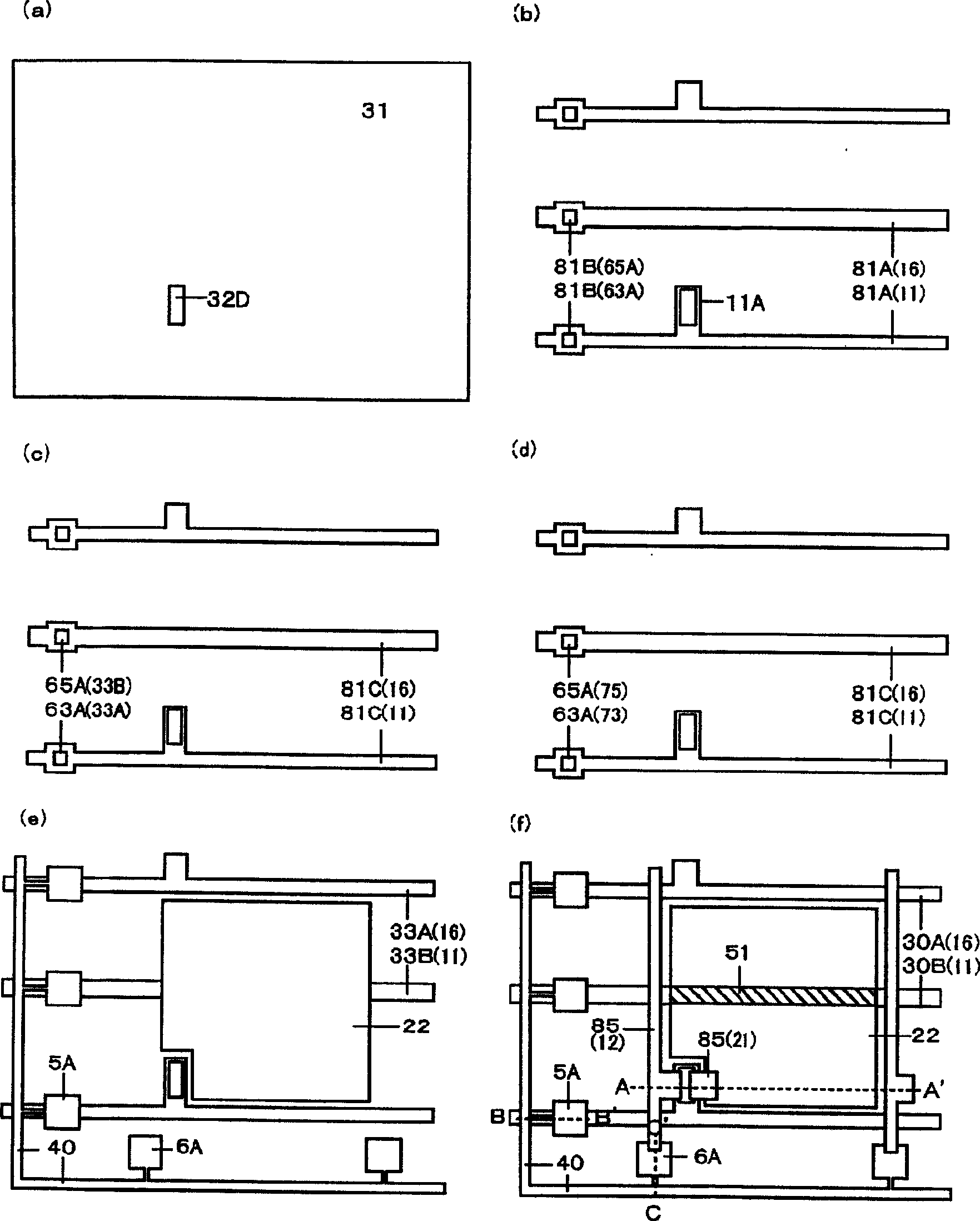
[0128] Next, the entire surface of the glass substrate 2 is covered with, for example, ITO as a transparent conductive layer with a film thickness of about 0.1 to 0.2 μm using a vacuum film forming apparatus such as SPT, and the image 3 (e) and Figure 4 As shown in (e), pixel electrodes 22 are selectively formed on the glass substrate 2 by microfabrication technology. At this time, in the area outside the image display portion, the scanning line electrode terminal 5 and the signal line electrode termina...

Embodiment 3

[0133] In Example 3, first, the main surface of the glass substrate 2 is coated with, for example, ITO and the first metal layer 92 with a film thickness of about 0.1 to 0.3 μm using a vacuum film forming apparatus such as SPT, as a film thickness of 0.1 to 0.2 μm. left and right transparent conductive layers 91 . In Embodiments 3 to 5, the scanning lines are stacked layers of a transparent conductive layer and a metal layer. Therefore, it is impossible to form an insulating layer on the side of the scanning lines during anodic oxidation, which will be clearly explained below. Here, the organic insulating layer is formed by electrodeposition in the insulating layer. Therefore, for example, high melting point metals such as Cr, Ta, Mo, or these alloys or silicides are selected as the first electrode that does not cause battery reaction with the transparent conductive layer ITO. 1 metal layer, used as scan line material. If Al is used for low resistance, a single layer such as ...


PUM

PropertyMeasurementUnit
Film thicknessaaaaaaaaaa

Abstract

To solve such a problem that in the conventional manufacturing method wherein the number of manufacturing steps is reduced, when a channel length is shortened, a manufacturing margin is small and a yield is lowered. A four sheet mask process and a three sheet mask process of TN type and IPS type liquid crystal display devices are constructed by combining technologies of a novel technology which first forms an etch stop layer and then rationalizes a scanning line forming step and a contact forming step by introducing a halftone exposure technology, a new technology which rationalizes a step for forming a protective layer of an electrode terminal by introducing a halftone exposure technology to an anodization step of a source/drain wiring which is a well-known technology, and a rationalization technology simultaneously forming a pixel electrode and a scanning line which is a well-known technology.

Description

[0001] technology area [0002] The invention relates to a liquid crystal display device with a color image display function, in particular to an active liquid crystal display device. Background technique [0003] With recent advances in microfabrication technology, liquid crystal material technology, and high-density mounting technology, liquid crystal display devices with a diagonal of 5 to 50 cm have been provided in large quantities as commercial bases for television images or various image display devices. Furthermore, color display can be easily realized by forming RGB colored layers in advance on one of the two glass substrates constituting the liquid crystal substrate. In particular, the so-called active type liquid crystal substrate, which has a built-in switching element in each pixel, has very little crosstalk, and ensures fast response and high contrast images. [0004] These liquid crystal display devices (liquid crystal substrates) generally have a matrix arrang...

Claims


Application Information

Patent Timeline
IPC IPC(8): G02F1/1368G02F1/133G02F1/136G09F9/30G09F9/35H01L21/00H01L21/3205H01L27/00
Inventor 川崎清弘
Owner AU OPTRONICS CORP
Why Eureka
Try Eureka