Light-emitting device and electronic device

A technology for light-emitting devices and light-emitting elements, which is applied in the fields of light-emitting materials, electric solid-state devices, semiconductor devices, etc., and can solve the problems of difficulty in achieving high added value

Active Publication Date: 2005-04-27
SEMICON ENERGY LAB CO LTD
View PDF0 Cites 9 Cited by
  • Summary
  • Abstract
  • Description
  • Claims
  • Application Information

AI Technical Summary

Problems solved by technology

In particular, the recent portable information terminals tend to be ...

Method used


Image

  • Light-emitting device and electronic device
  • Light-emitting device and electronic device
  • Light-emitting device and electronic device

Examples


Embodiment 1

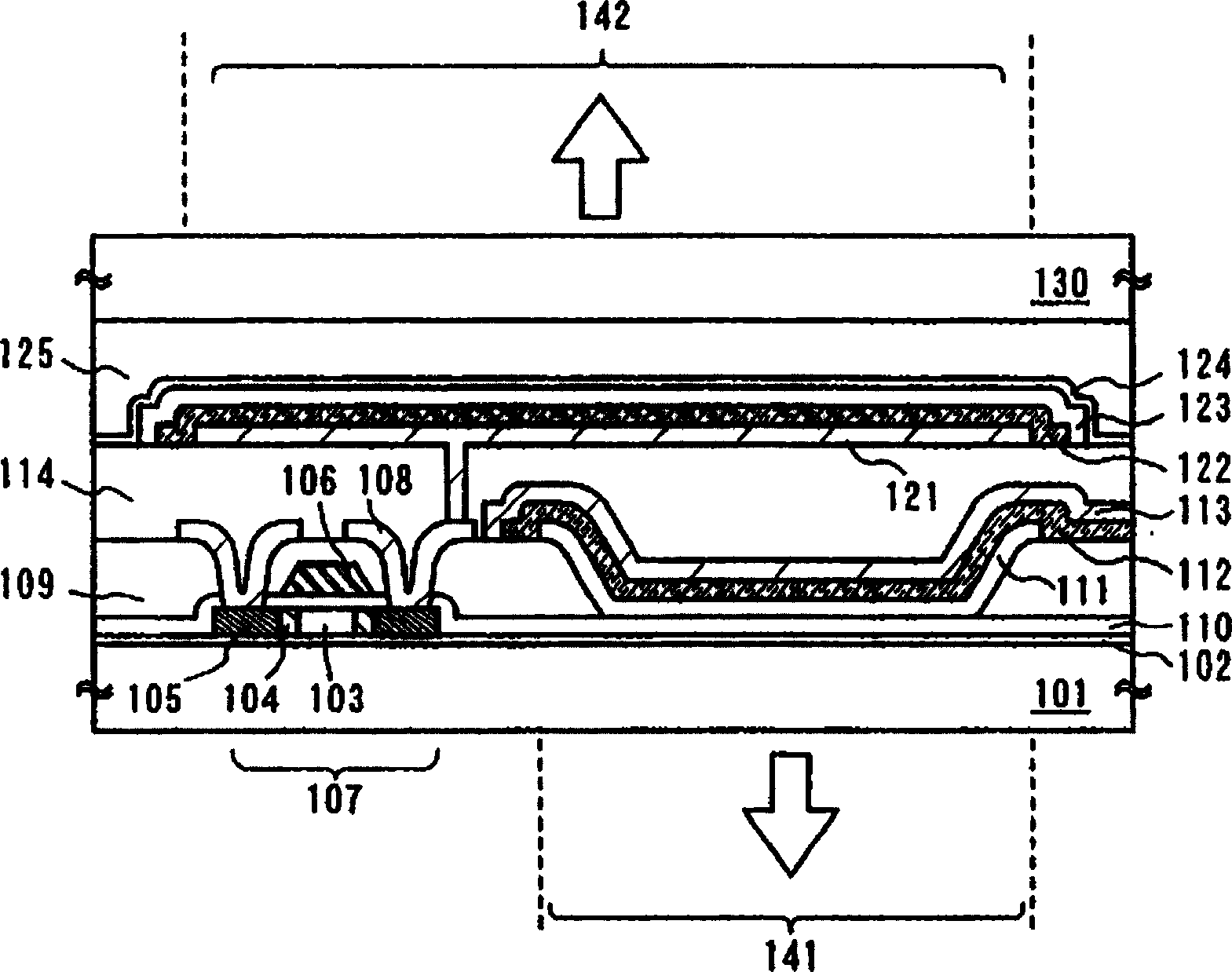
[0126] This example will use Figure 4A-Figure 7 The manufacturing process of the light-emitting element having the structure of Embodiment Mode 1 will be described.

[0127] Figure 4A and 4B represents a process of forming a first electrode of a first light-emitting element and a part of a TFT of a second light-emitting element, Figure 4A represents its top view, Figure 4B means along Figure 4A Sectional view of the A-A' line cut.

[0128] Such as Figure 4A As shown, an underlying insulating film 402 is formed on a glass substrate (first substrate 401). In this embodiment, the base insulating film has a two-layer structure, using SiH 4 , NH 3 , N 2 O is used as a reactive gas to form the first silicon oxynitride film with a thickness of 50-100nm; using SiH 4 , N 2 O is used as a reactive gas to form a second silicon oxynitride film with a thickness of 100-150 nm, and after stacking, a two-layer stack is formed.

[0129] Then, an amorphous silicon film is lami...

Embodiment 2

[0151] This embodiment will describe a structural example in which a light emitting device including at least a pixel portion, a driving circuit for driving a pixel, and a pixel processing circuit is formed on a substrate with an insulating surface, and an operation method for reducing power consumption.

[0152] Figure 11 Shown is an example of a system in which a display portion is formed on a glass substrate, on which a pixel portion 801, a source line driver circuit 802, a gate line driver circuit 803, three image processing circuits 804- 806, memory 807, interface circuit 808, power supply timing control circuit 809.

[0153] Figure 11 In the block diagram shown, a pixel portion 801 is a portion that displays an image; a source line driver circuit 802 and a gate line driver circuit 803 are driver circuits that drive pixels. Pixel data is input to the source line driver circuit 802 . In addition, the interface circuit 808 inputs external image data or image-based data...

Embodiment 3

[0162] An electronic device including the light-emitting device formed according to Embodiment Modes 1 to 5, Examples 1 and 2 will be described in this example. Typical examples include camcorders, digital cameras, notebook computers, portable information terminals (such as portable computers, mobile phones, portable game consoles or e-books), playback devices including recording media (specifically, devices capable of processing such as digital data on a recording medium such as a general-purpose disc (DVD) and has a display capable of displaying data images), television receivers, electronic bulletin boards, cash registers, etc. This embodiment shows an example in which the light-emitting device of the present invention is applied to a mobile phone.

[0163] Figures 9A to 9D It shows the external view of the mobile phone of the present invention, Figure 9A An oblique perspective view showing the open state, Figure 9B The oblique perspective view showing the folded stat...


PUM


Abstract

The present invention provides a light-emitting device whose volume is small and that has plural display screens, and a personal digital assistant that realizes higher added value by using the same. A light-emitting device of the present invention has a plurality of light-emitting elements in a pixel, and these light-emitting elements emit light in a different direction from each other and a pixel driving element is provided in one of the light-emitting elements. The light-emitting device can display in both front and back sides and independently display images on the both sides. Further, it can provide a higher aperture ratio, which is obtained by adding the aperture ratios of the both sides. Furthermore, it is also possible to see different images on the both sides of an electronic device using a display device of the present invention. Moreover, weight saving and thinning of electronic devices can be realized.

Description

technical field [0001] The present invention relates to a light-emitting device in which a pixel portion is formed by a light-emitting element, wherein the light-emitting element includes a light-emitting layer containing an Electro-Luminescence (Electro-Luminescence) substance between a pair of electrodes, and particularly relates to a light-emitting device that can be used in two Light-emitting devices displayed on the surface. Furthermore, the invention also relates to an electronic device comprising two display surfaces, a front and a rear. Background technique [0002] In recent years, electronic devices, especially portable information terminals (mobile computers, mobile phones, portable game machines, or electronic books) have been required to have high added value due to the diversification of their purposes. Recently, electronic devices that provide a sub-display surface on the back of a general display surface have appeared (see Patent Document 1). [0003] Resea...

Claims


Application Information

Patent Timeline
IPC IPC(8): H05B33/00C09K11/06G09G3/32H01L27/32H05B33/12H05B33/14H05B33/22H05B33/26H05B44/00
CPCH01L27/3267G09G2300/0439G09G2300/0809H01L27/3286G09G2300/0408G09G3/3225G09G3/3216G09G2300/0426H10K59/128H10K59/176H05B33/00H05B33/14
Inventor 濑尾哲史中岛晴惠根本幸惠
Owner SEMICON ENERGY LAB CO LTD
Why Eureka
Try Eureka