Highly integrable edge emitting active optical device and a process for manufacture of the same

a technology of active optical devices and manufacturing processes, applied in the field of semiconductors, can solve the problems of significant stress on the semiconductor, inefficient light-emitting materials of silicon, and the development of silicon active optical devices such as lasers and optical amplifiers, and achieve the effect of high temperature operation and lifetime of the devi

Inactive Publication Date: 2010-12-30
RUMPLER JOSEPH JOHN +1
View PDF1 Cites 39 Cited by
  • Summary
  • Abstract
  • Description
  • Claims
  • Application Information

AI Technical Summary

Benefits of technology

[0015]This invention relates to highly integrable electrically pumped continuous-wave III-V semiconductor edge emitting active optical devices, such as lasers, optical amplifiers and the like, and the process used to manufacture the same by a new approach enabling the production of platelet active optical devices with cleaved facets and precisely defined lengths. The technology allows for the use of a good thermally conducting material in the interface between the semiconductor active optical device and the substrate on which the device is ultimately integrated. This should have significant benefits for the high temperature operation and lifetime of the device. The process technology described is highly modular so that it can be applied to wide varieties of devices, materials, and substrates; it is also well suited for integrating lasers operating at different wavelengths on the same substrate.

Problems solved by technology

The development of silicon active optical devices like lasers and optical amplifiers, however, has proved to be much more challenging.
The difficulty lies in the fact that silicon is an inefficient light emitting material due to its indirect energy band gap.
Although these demonstrations represent tremendous breakthroughs, each of these approaches requires an additional laser to pump the devices and achieve light emission.
A common problem with this approach is that there are both lattice constant and thermal expansion coefficient mismatches between the III-V based semiconductor and silicon that result in significant stresses in the semiconductors.
With this approach, the thermal expansion coefficient mismatch is a common problem since the bonding occurs at elevated temperatures.
Unfortunately, these techniques can locate the cleave position to a precision of no better than 5 microns (See, e.g., Marsh et al., J. of Crystal Growth, 288, Iss. 1, 2-6 (2006)), which severely hampers control of the laser cavity length.
The more difficult challenge with the coaxial coupling integration strategy is the accurate and consistent dimensioning of the length of the edge emitting laser which allows the gap between the laser and waveguide facets to be kept small.
An additional problem with conventional cleaving methods is that the mechanical nature of these cleaving processes does not allow for reliable cleaving of thin-film semiconductors (i.e., tens of microns or thinner).
The main drawback with facet etching, though, is that unlike cleaving, etching seems to invariably impart roughness on the facets and does not result in an ideal facet.

Method used


Image

  • Highly integrable edge emitting active optical device and a process for manufacture of the same
  • Highly integrable edge emitting active optical device and a process for manufacture of the same
  • Highly integrable edge emitting active optical device and a process for manufacture of the same

Examples


Embodiment Construction

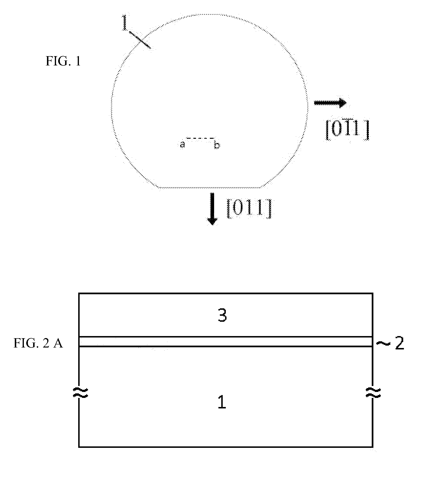
[0047]In the following, an embodiment of the semiconductor edge emitting laser platelet process in accordance with the present invention will be explained with reference to the accompanying figures. The description herein refers to the use of Indium Phosphide as the material from which the laser is manufactured. This technology applies equally well to other materials, such as Gallium Arsenide, that have a similar crystal structure.

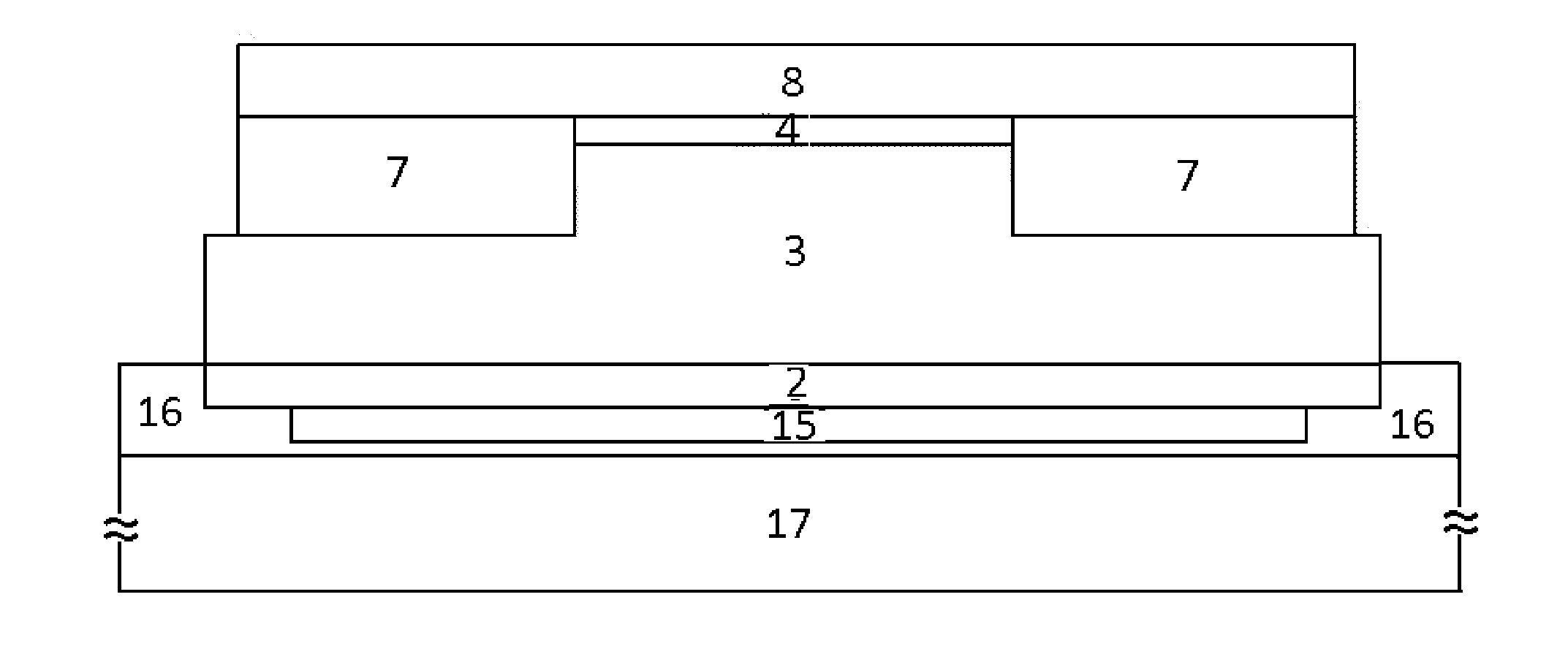
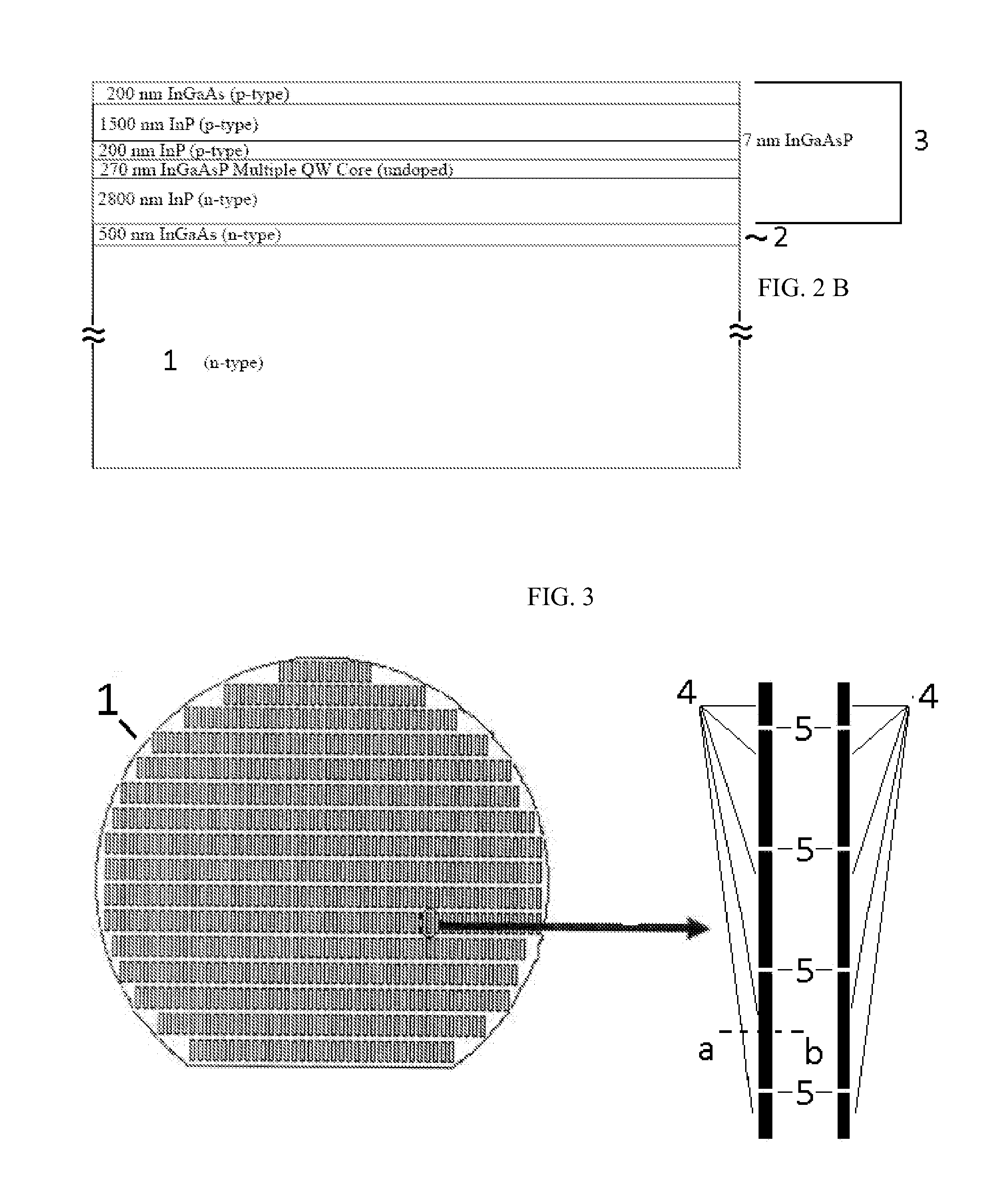
[0048]FIG. 1 is a view of the (100)-oriented InP wafer 1 (which is hundreds of microns thick) upon which has been grown an edge emitting laser epitaxial structure. The wafer crystal orientation is chosen since the cleavage planes lie along the (011) and (011) planes, or in other words, the orthogonal directions on a (100)-oriented wafer. FIG. 2A is a view of the cross section of the wafer shown in FIG. 1 taken along the line a-b. Between the semiconductor laser layer structure 3 and the InP substrate, there is a thin (i.e., a few hundred to several hundred...


PUM


Abstract

Described herein is a novel technique used to make novel thin III-V semiconductor cleaved facet edge emitting active optical devices, such as lasers and optical amplifiers. These fully processed laser platelets with both top side and bottom side electrical contacts can be thought of as freestanding optoelectronic building blocks that can be integrated as desired on diverse substrates for a number of applications, many of which are in the field of communications. The thinness of these platelets and the precision with which their dimensions are defined using the process described herein makes it conducive to assemble them in dielectric recesses on a substrate, such as silicon, as part of an end-fire coupled, coaxial alignment optoelectronic integration strategy. This technology has been used to integrate edge emitting lasers onto silicon substrates, a significant challenge in the field of silicon optoelectronics.

Description

CROSS-REFERENCE TO RELATED APPLICATIONS[0001]This patent application claims benefit of prior U.S. Provisional Patent Application Ser. No. 61 / 222,020, filed Jun. 30, 2009 by Joseph J. Rumpler et al. for HIGHLY INTEGRABLE EDGE EMITTING ACTIVE OPTICAL DEVICE AND A PROCESS FOR MANUFACTURE OF THE SAME.STATEMENT REGARDING FEDERALLY SPONSORED RESEARCH OR DEVELOPMENT[0002]Not Applicable.REFERENCE TO SEQUENCE LISTING, A TABLE, OR A COMPUTER PROGRAM LISTING COMPACT DISC APPENDIX[0003]Not Applicable.BACKGROUND OF THE INVENTION[0004]The present invention is in the technical field of semiconductors. In particular, this invention relates to highly integrable edge emitting active optical devices such as lasers, optical amplifiers and the like, and the manufacture of the same.[0005]For over forty years, silicon has been the material of choice for high density microelectronics in large part because of the performance advantages of high speed, low static power complementary metal oxide semiconductor ...

Claims


Application Information

Patent Timeline
Patent Type & Authority Applications(United States)
IPC IPC(8): H01S5/20H01L21/30H01S5/50
CPCB82Y20/00H01S5/0201H01S5/0202H01S5/021H01S5/0216H01S5/50H01S5/3434H01S5/3202H01S5/0206H01S5/3013H01S5/0217
Inventor RUMPLER, JOSEPH JOHNFONSTAD, CLIFTON G.
Owner RUMPLER JOSEPH JOHN
Why Eureka
Try Eureka