Semiconductor devices having different gate dielectrics and methods for manufacturing the same

一种栅极介质、半导体的技术,应用在半导体/固态器件制造、半导体器件、电固体器件等方向,达到阈值电压操作快速和可靠、减少负面影响、高速运行漏电流的效果

Active Publication Date: 2005-05-25
SAMSUNG ELECTRONICS CO LTD
View PDF0 Cites 15 Cited by
  • Summary
  • Abstract
  • Description
  • Claims
  • Application Information

AI Technical Summary

Problems solved by technology

These traps have an adverse effect on the threshold voltage (Vt) characteristics of PMOS and NMOS devices

Method used


Image

  • Semiconductor devices having different gate dielectrics and methods for manufacturing the same
  • Semiconductor devices having different gate dielectrics and methods for manufacturing the same
  • Semiconductor devices having different gate dielectrics and methods for manufacturing the same

Examples


Embodiment Construction

[0025] The invention will now be described in the form of several preferred but not limiting embodiments with reference to the accompanying drawings. It should be noted that the relative dimensions shown in the drawings are not to scale with the actual dimensions.

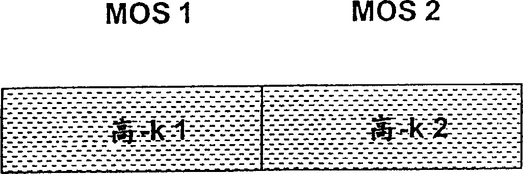
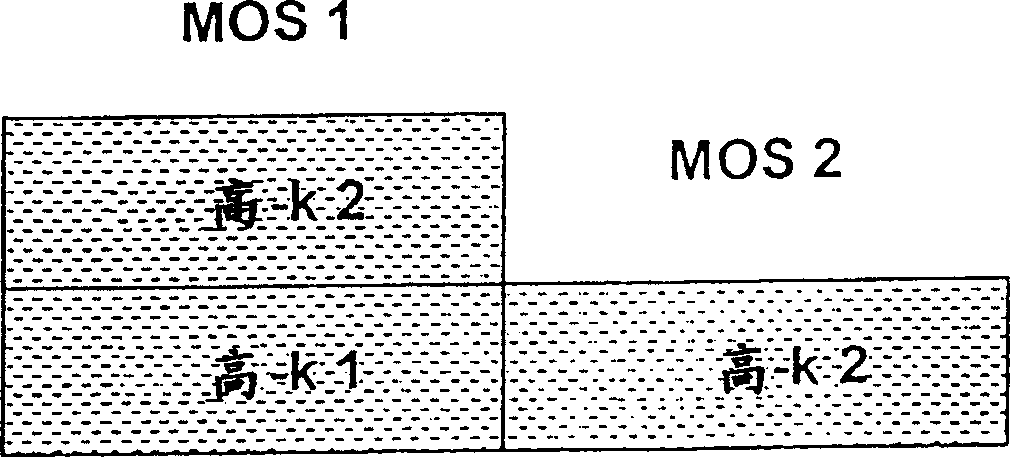
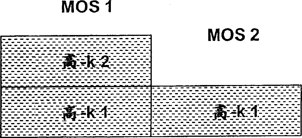
[0026] 1(A), 1(B) and 1(C) are simplified schematic diagrams of embodiments of gate dielectrics used in MOS devices according to the present invention.

[0027] FIG. 1(A) shows a gate dielectric of a semiconductor device including a first type metal oxide semiconductor (MOS1) and a second type metal oxide semiconductor device (MOS2). In some embodiments, MOS1 is an n-channel metal oxide semiconductor (NMOS) device, and MOS2 is a p-channel metal oxide semiconductor (PMOS) device. In other embodiments, MOS1 is a PMOS device, and MOS2 is an NMOS device. In the embodiment of FIG. 1(A), the gate dielectric of MOS1 is a first high-k dielectric material (high k1 ), and the gate dielectric of MOS2 is a second high-k diel...


PUM


Abstract

A semiconductor device includes first and second transistor devices. The first device includes a first substrate region, a first gate electrode, and a first gate dielectric. The first gate dielectric is located between the first substrate region and the first gate electrode. The second device includes a second substrate region, a second gate electrode, and a second gate dielectric. The second gate dielectric is located between the second substrate region and the second gate electrode. The first gate dielectric includes a first high-k layer having a dielectric constant greater than or equal to 8. Likewise, the second gate dielectric includes a second high-k layer having a dielectric constant greater than or equal to 8. The second high-k layer has a different material composition than the first high-k layer.

Description

technical field [0001] The present invention relates generally to transistor devices, and in particular to devices having transistors each comprising different high-k gate dielectrics, and processes for forming such devices. Background technique [0002] Conventional transistor devices, such as metal-oxide-semiconductor (MOS) devices, are characterized by a silicon dioxide (SiO2) interposed between the gate electrode and the channel region. 2 ) of the gate dielectric. The performance of such devices can be improved by increasing the capacitance between the gate electrode and the channel region, and a common way to increase capacitance is to reduce the SiO 2 The thickness of the gate dielectric is below 100 Angstroms. In fact, today gate dielectrics are nearly 40 Angstroms thick. Unfortunately, however, above and below this thickness, using SiO 2 It has limitations as a gate dielectric. This is because in SiO 2 Dielectrics less than approximately 40 angstroms in the cas...

Claims


Application Information

Patent Timeline
Patent Type & Authority Applications(China)
IPC IPC(8): H01L21/8234H01L21/8238H01L27/092H01L29/78
CPCH01L21/823857H01L27/0922
Inventor 李钟镐姜虎圭丁炯硕都昔柱金润奭
Owner SAMSUNG ELECTRONICS CO LTD
Why Eureka
Try Eureka