Solid-state imaging device and manufacturing method thereof

A technology for a solid-state imaging device and a manufacturing method, which can be applied to electric solid-state devices, semiconductor devices, electrical components, etc., and can solve the problems of rising absorptivity, difficulty in concentrating light, and burying of recesses by resins, etc.

Inactive Publication Date: 2005-06-08
PANASONIC CORP
View PDF1 Cites 17 Cited by
  • Summary
  • Abstract
  • Description
  • Claims
  • Application Information

AI Technical Summary

Problems solved by technology

[0014] The miniaturization of the unit pixel is related to the reduction of the opening width of the photodiode 1 as the opening of the light-shielding film 6. There are also cases where the film thickness of the vertical transfer gate 3 and the reduction ratio of the opening width cannot be thinned. A narrow vertical pit-like structure is formed, so it is difficult to achieve the concentration of incident light
[0015] In addition, shortening the exit pupil distance of the camera lens means that the ratio of the angle of the incident light incident on the solid-state imaging device deviated from the vertical direction increases, so it is difficult to effectively condense the incident light onto the photodiode 1.
[0016] In addition, according to the technology disclosed in Japanese Patent No. 2869280, although the water-soluble resin is applied and the upper part is covered with other resin, and then the water-soluble resin is dissolved to form the gas layer, but fo

Method used


Image

  • Solid-state imaging device and manufacturing method thereof
  • Solid-state imaging device and manufacturing method thereof
  • Solid-state imaging device and manufacturing method thereof

Examples


no. 1 approach

[0057] Figure 5 It is a schematic diagram showing the cross-sectional structure of the solid-state imaging device according to the first embodiment of the present invention.

[0058] exist Figure 5 Among them, the solid-state imaging device 51 includes: a photodiode 1 having a photoelectric conversion function, a vertical transfer part 2 of an embedded channel structure that transfers signal charges to a vertical direction, a vertical transfer grid 3 that controls vertical transfer, and is used to make the incident Light is incident on the photodiode 1 and is not incident on the light-shielding film 6 of other areas such as the vertical transport section 2, and is made of SiO 2 The dielectric films 81, 82 and 83 as the main components, the dielectric film 21 with SiON as the main component, the protective film 10, and the organic dielectric film 12 with both planarization and color filtering functions are used to condense the incident light to the photoelectric A lens 7 fo...

no. 2 approach

[0077] Figure 7 It is a schematic diagram showing the cross-sectional structure of the solid-state imaging device according to the second embodiment of the present invention.

[0078] In the solid-state imaging device according to the second embodiment, the dielectric film 21 is also formed on the upper part of the photodiode 1. The difference from the first embodiment is that the dielectric film 21 and the photodiode 1 are formed on the upper part of the Si substrate 11 interface. SiO 2 Multilayer structure of film 82 .

[0079] like Figure 7 As shown, the solid-state imaging device 52 includes: a photodiode 1, a vertical transfer section 2, a vertical transfer grid 3, and a light-shielding film 6 for making incident light incident on the photodiode 1 and not incident on other areas such as the vertical transfer section 2. , with SiO 2 Dielectric films 81, 82, and 83 as main components, dielectric film 21 mainly composed of SiON, protective film 10, and organic dielectr...

no. 3 approach

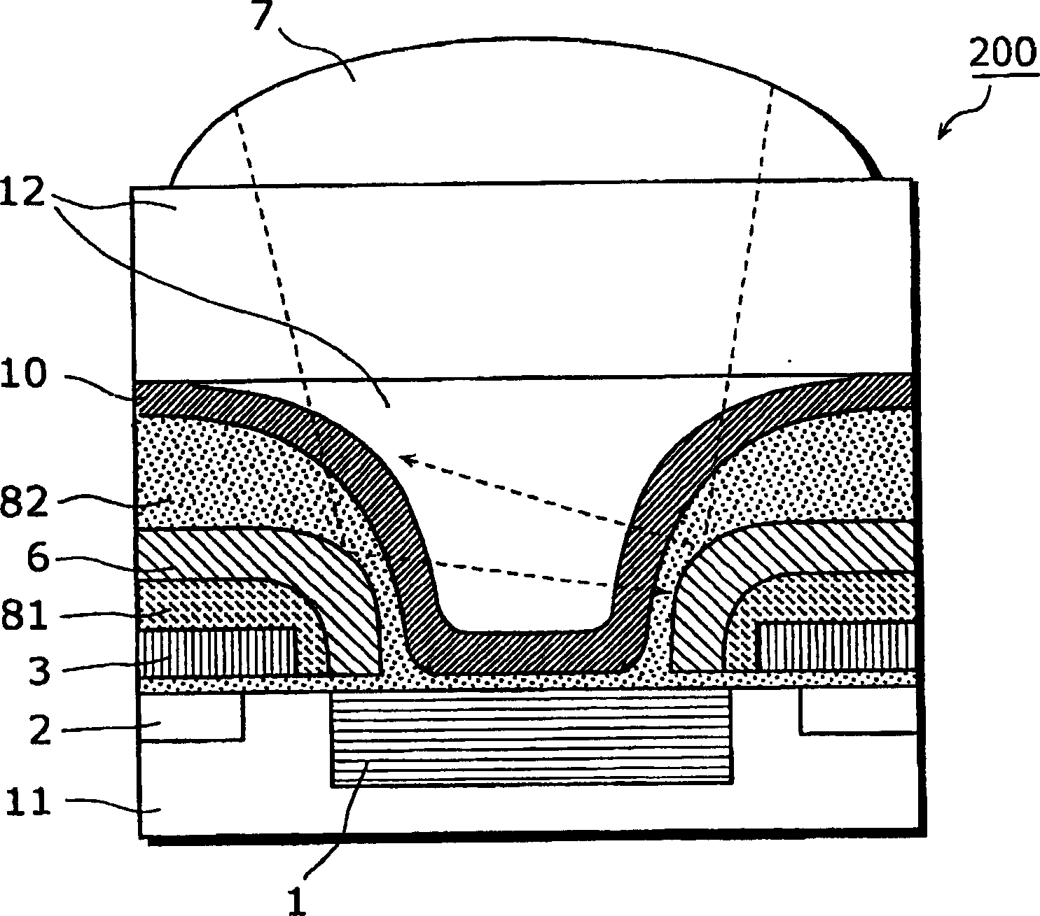
[0100] Figure 9 It is a schematic diagram showing the cross-sectional structure of the solid-state imaging device according to the third embodiment of the present invention.

[0101] like Figure 9 As shown, a unit pixel 201 includes: a photodiode 1 formed in a silicon substrate 11 with a photoelectric conversion function; a vertical transfer part 2 of an embedded channel structure that transfers signal charges to a vertical direction; a vertical transfer gate that controls vertical transfer pole 3; formed on the upper part of the vertical transfer gate 3, made of SiO 2 A dielectric film 81 as the main component; a light-shielding film 6 formed on the top of the dielectric film 81 and used to prevent incident light from entering areas such as the vertical transport portion 2 and the vertical grid 3; of SiO 2 The dielectric film 82 that is the main component; only the portion of the dielectric film 82 that is opposed to the opening of the photodiode 1 is connected, and the ...


PUM

PropertyMeasurementUnit
Melting pointaaaaaaaaaa

Abstract

The invention provides a solid-state imaging device, comprising: a photodiode (1) that converts incident light into charges, a first dielectric film (82) formed on the upper part of the photodiode (1), and The second dielectric film (83) and the third dielectric film (21) formed on the top of ), the hollow layer (9) provided between any of the first to third dielectric films.

Description

technical field [0001] The present invention relates to a solid-state imaging device capable of being mounted in a digital camera, an integrated video camera, etc., and a method of manufacturing the same. Background of the invention [0002] In recent years, solid-state imaging devices have been widely provided for use in integrated video cameras, imaging sections of digital cameras, and the like. Among them, a CCD-type solid-state imaging device of an interline transfer method (hereinafter referred to as an IT-CCD) has attracted attention in particular because of its low-noise characteristics. [0003] figure 1 It is a schematic diagram showing the structure of a conventional IT-CCD. [0004] like figure 1 As shown, the solid-state imaging device 100 includes: a photodiode 1 having a photoelectric conversion function, a vertical transfer part 2 with an embedded channel structure that transfers signal charges to the vertical direction, a vertical transfer gate 3 that cont...

Claims


Application Information

Patent Timeline
IPC IPC(8): H01L27/14H01L27/146H01L27/148H04N5/335
CPCH01L27/14658H01L27/14621H01L27/14625H01L27/14683
Inventor 加藤良章
Owner PANASONIC CORP
Why Eureka
Try Eureka