Electronic device, display device and production method thereof
A technology for electronic components and display components, applied in electrical components, semiconductor/solid-state device manufacturing, electrical solid-state devices, etc., can solve problems such as short circuit of conductive layers and lower yield
- Summary
- Abstract
- Description
- Claims
- Application Information
AI Technical Summary
Problems solved by technology
Method used
Image

Examples
no. 1 approach
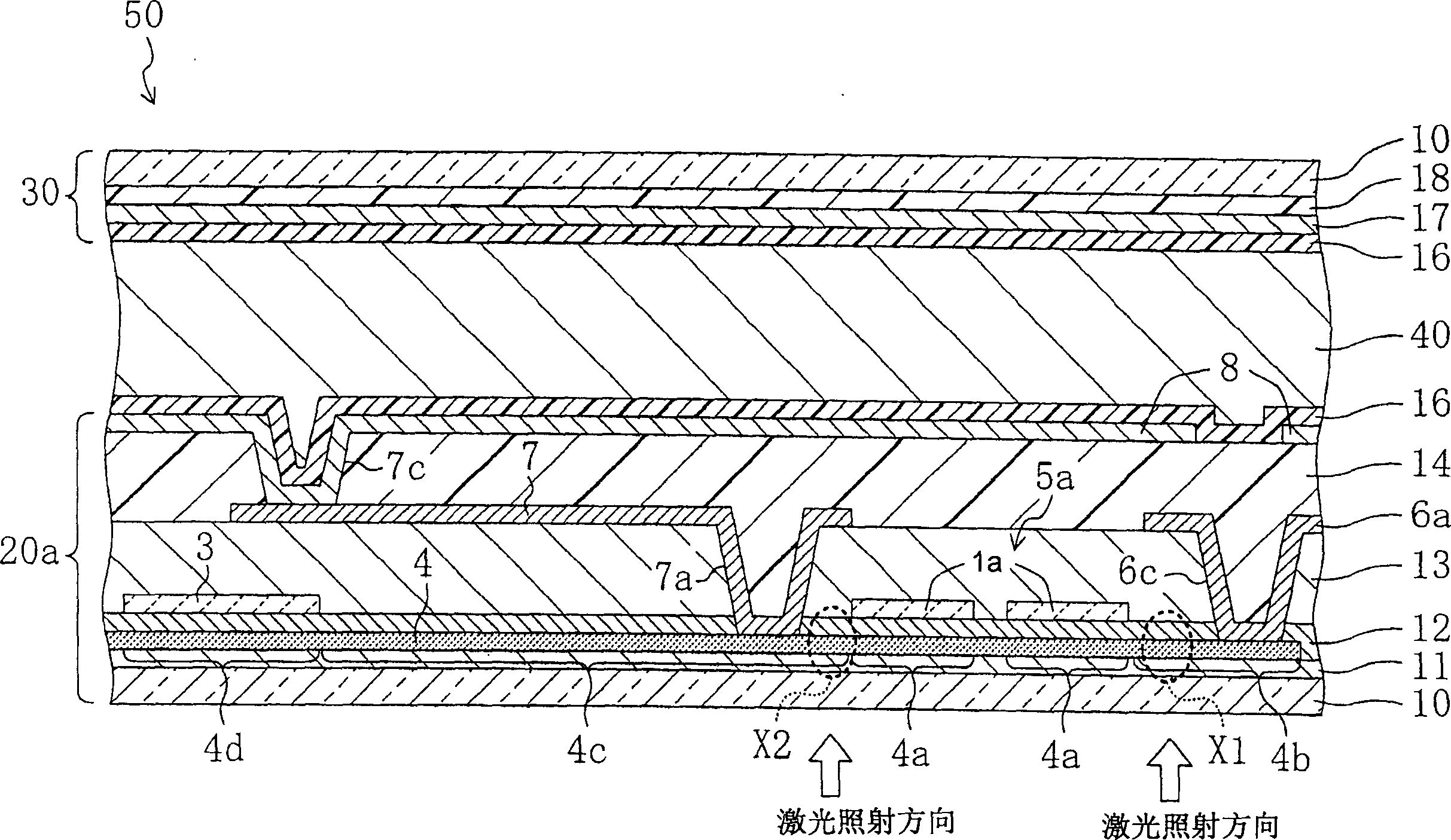
[0277] Next, the liquid crystal display device 50 according to the first embodiment of the present invention will be described.
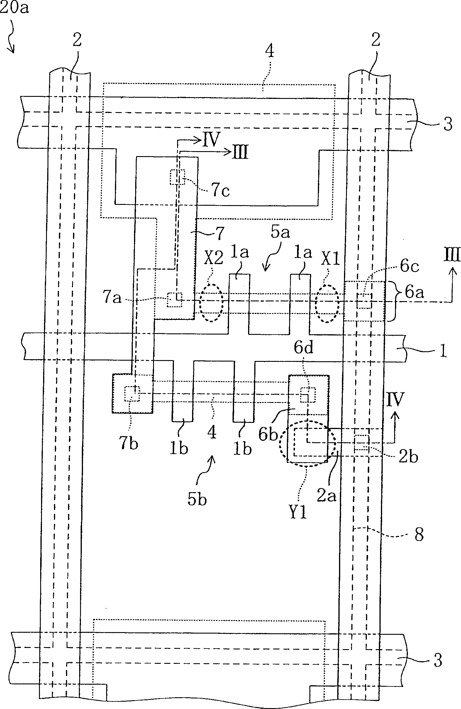
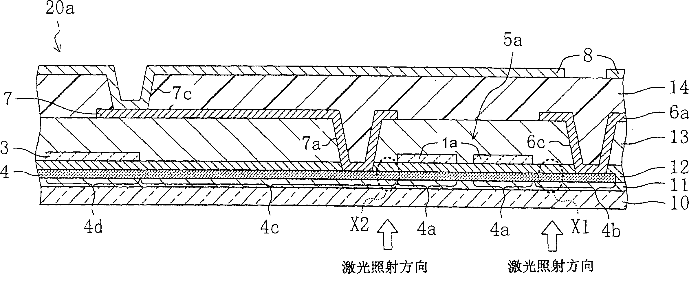
[0278] figure 1is a schematic cross-sectional view of a liquid crystal display device 50, figure 2 is a schematic plan view of the active matrix substrate 20a constituting the liquid crystal display device 50, image 3 is corresponding to figure 2 A schematic cross-sectional view of the active matrix substrate 20a in section III-III, Figure 4 is corresponding to figure 2 A schematic cross-sectional view of the active matrix substrate 20a of the section IV-IV in FIG.
[0279] The liquid crystal display device 50 is provided with an active matrix substrate 20 a , a counter substrate 30 facing thereto, and a liquid crystal layer 40 provided between the two substrates 20 a and 30 .
[0280] In the active matrix substrate 20a, as figure 2 As shown in , on an insulating substrate 10, a plurality of gate lines 1 and a plurality of source lines ...
no. 2 approach
[0349] Next, a liquid crystal display device according to a second embodiment of the present invention will be described. Furthermore, in each of the following embodiments, for Figure 1 to Figure 6 The same reference numerals are given to the same parts, and detailed description thereof will be omitted.
[0350] Figure 7 is a schematic plan view of an active matrix substrate 20b constituting a liquid crystal display device, Figure 8 is corresponding to Figure 7 A schematic cross-sectional view of the active matrix substrate 20b of the section VIII-VIII in FIG. Furthermore, because Figure 7 The cross-sectional composition of the active matrix substrate 20b at the section III-III in image 3 The cross-sectional structure of the active matrix substrate 20a is substantially the same, so the schematic cross-sectional view is omitted.
[0351] This liquid crystal display device is provided with an active matrix substrate 20b, a counter substrate opposed thereto, and a liq...
no. 3 Embodiment approach
[0377] The liquid crystal display device of the present invention may also have the following configuration in the first embodiment described above.
[0378] Figure 10 is a schematic plan view of an active matrix substrate 20c constituting a liquid crystal display device, Figure 11 is corresponding to Figure 10 A schematic cross-sectional view of the active matrix substrate 20c in the section XI-XI, Figure 12 is corresponding to Figure 10 A schematic cross-sectional view of the active matrix substrate 20c of the section XII-XII in FIG.
[0379] This liquid crystal display device includes an active matrix substrate 20c, a counter substrate facing the active matrix substrate, and a liquid crystal layer interposed between these two substrates.
[0380] active matrix substrate 20c, such as Figure 11 As shown in , the composition of the laminated film from the base cover film 11 to the pixel electrode 8 is substantially the same as that of the active matrix substrate 20a...
PUM
| Property | Measurement | Unit |
|---|---|---|
| coating thickness | aaaaa | aaaaa |
Abstract
Description
Claims
Application Information
 - R&D
- Intellectual Property
- Life Sciences
- Materials
- Tech Scout
- Unparalleled Data Quality
- Higher Quality Content
- 60% Fewer Hallucinations
Browse by: Latest US Patents, China's latest patents, Technical Efficacy Thesaurus, Application Domain, Technology Topic, Popular Technical Reports.
© 2025 PatSnap. All rights reserved.Legal|Privacy policy|Modern Slavery Act Transparency Statement|Sitemap|About US| Contact US: help@patsnap.com