Method for realizing bar array semiconductor laser shaping by means of reflecting prism stack

A technology of lasers and semiconductors, applied in the direction of semiconductor lasers, lasers, laser components, etc., can solve the problems of inconvenient adjustment and mechanical parts design, unfavorable cost, and inconvenient adjustment, so as to achieve the promotion of the method and the cost. The effect of reducing and adjusting is convenient

Inactive Publication Date: 2005-09-07
INST OF OPTICS & ELECTRONICS - CHINESE ACAD OF SCI
View PDF0 Cites 11 Cited by
  • Summary
  • Abstract
  • Description
  • Claims
  • Application Information

AI Technical Summary

Problems solved by technology

For example, the stepped mirror deflects the optical axis of the system twice by 90 degrees, causing the shaping elements to be independent of each other in space, which brings inconvenience to the adjustment and mechanical design; the shaping method of the prism group catadioptric reflection deflects the direction of the optical axis More, there is also the problem of inconvenient adjustment; the micro-chip prism stack not only requires considerable prism processing accuracy, but also requires considerable alignment and gluing accuracy between prisms, which is not conducive to cost reduction

Method used


Image

  • Method for realizing bar array semiconductor laser shaping by means of reflecting prism stack
  • Method for realizing bar array semiconductor laser shaping by means of reflecting prism stack
  • Method for realizing bar array semiconductor laser shaping by means of reflecting prism stack

Examples


Embodiment 1

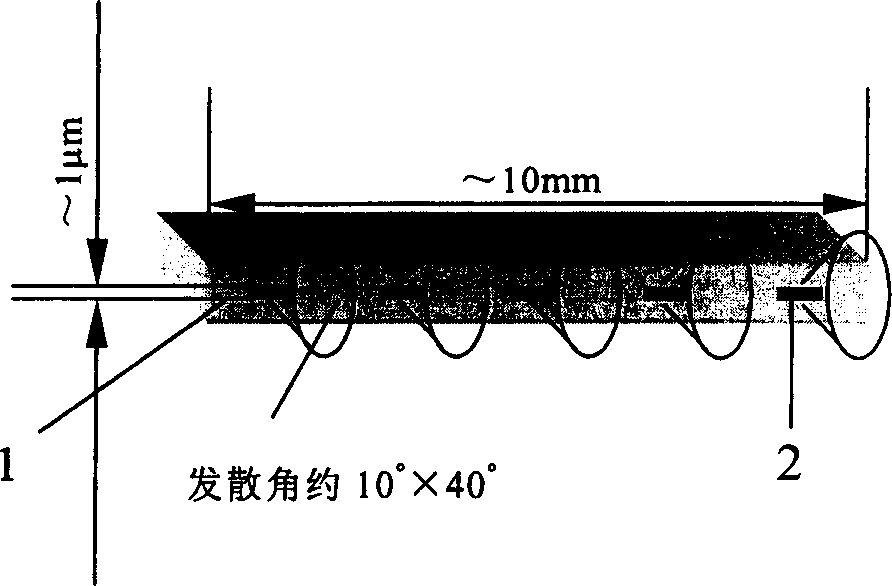
[0025] The strip semiconductor laser designed by the method of the present invention realizes the shaping process coupled with 800 μm core diameter, 0.37 numerical aperture optical fiber, and its design process is as follows:

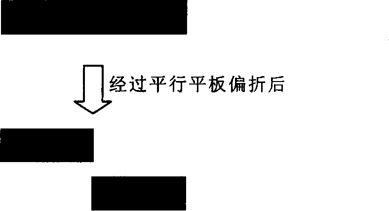
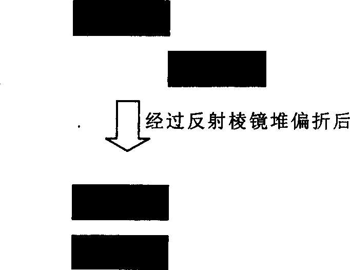
[0026] (1) In this embodiment, after the fast and slow axes of the strip semiconductor laser are collimated, the spot size in the slow axis direction is about 10mm, and the slow axis spot is deflected twice by a catadioptric prism stack, and aligned along the fast axis direction. The shaping system needs a reflective prism stack composed of a parallel plate and two reflective prisms. For the laser wavelength of 808nm, you can choose cheap K9 glass to make a parallel plate. Because the slow axis beam has a certain divergence, the length of the parallel plate is selected as 7mm. If the laser is 7.5mm away from the base, the height of the parallel plate can be chosen to be 12mm. In this example, the width of the parallel plate is selected as 5mm. In orde...

Embodiment 2

[0033] (1) In this embodiment, after the fast and slow axes of the strip semiconductor laser are collimated, the spot size in the slow axis direction is about 10mm, and the slow axis spot is deflected three times by using a catadioptric prism stack, and aligned along the fast axis direction. The shaping system requires a reflective prism stack composed of two parallel flat plates and three reflective prisms. As in the first embodiment, the parallel plate is made of K9 glass, and the length of the parallel plate is selected as 4 mm because the slow-axis light beam has a certain divergence. If the laser is 7.5mm away from the base, the height of the parallel plate can be chosen to be 12mm. In this example, the width of the parallel plate is selected as 5mm. In order to ensure that the light spots in the fast axis direction are as compact as possible without overlapping, the distance between the centers of the two light spots in this direction is selected as 1mm. The height of ...


PUM

PropertyMeasurementUnit
heightaaaaaaaaaa
heightaaaaaaaaaa

Abstract

This invention relates to method for shaping the strip semi-conductive laser by using the refracting and reflecting prism stack, which is characterized by the following: (1) using one or several parallel plats to split slow axial light spot of the strip semi-conductive laser; (2) using a group of stepwise reflecting prism stacks to align the splitting spots along the fast axial for the purpose of shaping the light beam.

Description

Technical field [0001] The invention relates to a method for realizing the shaping of a striped semiconductor laser by using a fold-reflective prism stack. Background technique [0002] High-power semiconductor lasers (Laser Diode, LD) with pigtail output have been widely used in medical treatment, material processing, pumping of solid-state lasers and fiber lasers, military, printing and printing, etc. Bar array semiconductor lasers (LD bar) are composed of a series of light-emitting units arranged periodically in the horizontal direction. However, due to limitations in technology, cooling, and shaping methods, it is impossible for bar array semiconductor lasers to be infinitely long in the horizontal direction. Therefore, the current strip semiconductor laser is generally about 1cm long, and the continuous output power is generally lower than 100W. [0003] The main characteristics of the output beam of semiconductor lasers are that in the horizontal direction (customaril...

Claims


Application Information

Patent Timeline
Patent Type & Authority Applications(China)
IPC IPC(8): G02F1/35H01S5/00
Inventor 郑国兴杜春雷周崇喜
Owner INST OF OPTICS & ELECTRONICS - CHINESE ACAD OF SCI
Why Eureka
Try Eureka