Non-volatile memory location and producing method thereof

A technology of non-volatile storage and manufacturing method, applied in semiconductor/solid-state device manufacturing, electrical components, electrical solid-state devices, etc., to achieve the effects of increasing component integration, increasing effective channel length, and simple process

Inactive Publication Date: 2005-09-28
POWERCHIP SEMICON CORP
View PDF0 Cites 5 Cited by
  • Summary
  • Abstract
  • Description
  • Claims
  • Application Information

AI Technical Summary

Problems solved by technology

[0006] In addition, due to the increasing size of computer application software, the required memory capacity is also increasing. For this situation where the size of the me

Method used


Image

  • Non-volatile memory location and producing method thereof
  • Non-volatile memory location and producing method thereof
  • Non-volatile memory location and producing method thereof

Examples


Embodiment Construction

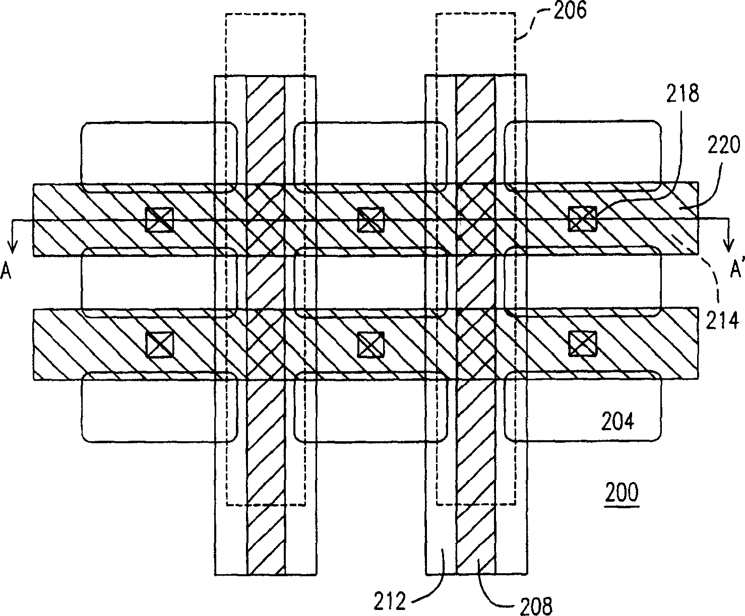
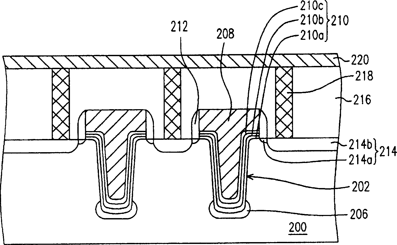
[0036] Figure 2A What is shown is a top view of a non-volatile memory unit according to a preferred embodiment of the present invention. Figure 2B Shown is a schematic cross-sectional view of a non-volatile storage unit in a preferred embodiment of the present invention, and it is Figure 2A Schematic cross-section along A-A'.

[0037] Please also refer to Figure 2A and Figure 2B, the non-volatile memory cell includes a substrate 200, an element isolation structure 204, a source / drain region 206, a gate 208, a composite dielectric layer 210, a spacer 212, a source / drain region 214, an interlayer dielectric Electrical layer 216 , plug 218 , wire 220 .

[0038] The substrate 200 is, for example, a silicon substrate, and a trench 202 is disposed in the substrate 200 . The device isolation structure 204 is disposed in the substrate 200 to define an active region. The element isolation structure 204 is, for example, a field oxide isolation structure or a shallow trench is...


PUM


Abstract

A non- volatile storage cell is composed of substrate, grid, the first source electrode / drain electrode area, composite dielectric layer and the second source electrode / drain electrode area. It is featured as setting a slot on substrate; placing grid in slot, the first source electrode / drain electrode area at slot bottom; setting composite dielectric layer between grid and slot surface and placing the second source electrode / drain electrode area in substrate at two side of grid.

Description

technical field [0001] The present invention relates to a semiconductor memory element, and in particular to a non-volatile memory cell (non-volatile memory cell) and a manufacturing method thereof. Background technique [0002] Among all kinds of non-volatile memory products, it has the advantages of multiple data storage, reading, erasing, etc., and the stored data will not disappear after power off. Programmable read-only memory (EEPROM) has become a storage element widely used in personal computers and electronic equipment. A typical electrically erasable and programmable read-only memory is made of doped polysilicon (floating gate) and control gate (control gate). When the memory is programmed, electrons injected into the floating gate are uniformly distributed throughout the polysilicon floating gate layer. However, when there are defects in the tunneling oxide layer under the polysilicon floating gate layer, it is easy to cause leakage current of the device and affe...

Claims


Application Information

Patent Timeline
IPC IPC(8): H01L21/8239H01L21/8247H01L27/105H01L27/115
Inventor 张格荥黄丘宗
Owner POWERCHIP SEMICON CORP
Why Eureka
Try Eureka