Light emitting device and fabrication method thereof and light emitting system using the same

A technology for light-emitting devices and light-emitting elements, applied in the field of light-emitting systems, can solve problems such as difficulty in production, increased cost, and complex structure.

Inactive Publication Date: 2005-10-19
LG ELECTRONICS INC
View PDF0 Cites 15 Cited by
  • Summary
  • Abstract
  • Description
  • Claims
  • Application Information

AI Technical Summary

Problems solved by technology

As a result, its structure becomes complicated and di

Method used


Image

  • Light emitting device and fabrication method thereof and light emitting system using the same
  • Light emitting device and fabrication method thereof and light emitting system using the same
  • Light emitting device and fabrication method thereof and light emitting system using the same

Examples


Embodiment approach

[0031] The light-emitting device according to the present invention can be implemented in various ways, and its preferred

[0032] Example.

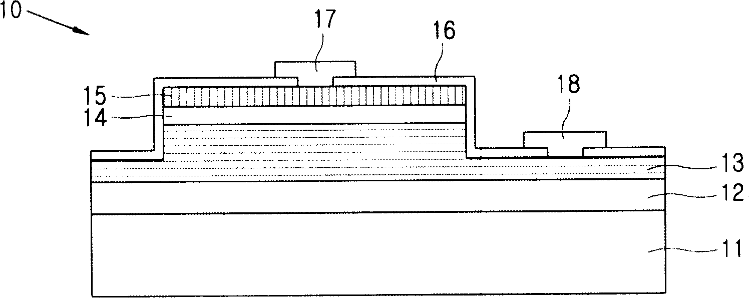
[0033] figure 2 is a cross-sectional view of the light emitting device according to the first embodiment of the present invention.

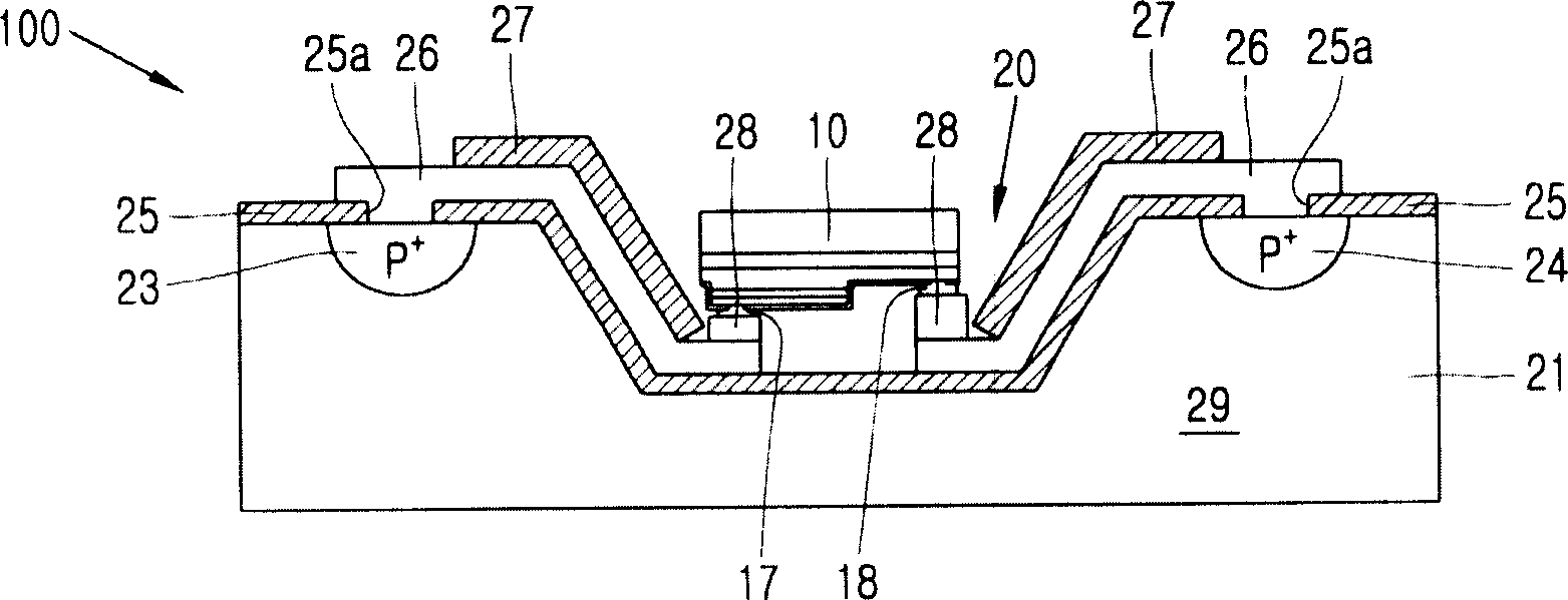
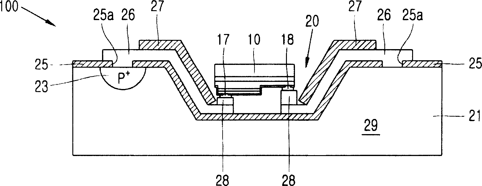
[0034] As shown in the figure, a light emitting device 100 according to a first embodiment of the present invention includes a light emitting element 10 having a first electrode 17 and a second electrode 18, and a cavity 20 having a light emitting element 10 mounted therein on its main surface and The semiconductor component 21 is electrically connected to the light emitting element 10 .

[0035] The depth of the hole 20 is preferably greater than the height of the light emitting device 10 so that the light emitted by the light emitting element 10 will not affect other elements and the overall size of the light emitting device 100 can be minimized.

[0036] The semiconductor member 21 is made of a silic...


PUM


Abstract

A light emitting device comprises a light emitting element having a first electrode and a second electrode, and a semiconductor member having a cavity in a principal surface thereof, inside which the light emitting element is mounted, and electrically connected to the light emitting element, wherein the semiconductor member is constructed as a voltage regulating diode for stabilizing a voltage supplied from the exterior. As a result, the light emitting element can be protected from a static electricity or a surge voltage flowed therein from the exterior, the entire size of the system can be remarkably reduced so as to simplify a structure thereof, and heat generated from the system can be effectively discharged to the exterior. In addition, by providing a reflection portion in the cavity, light emitted from the light emitting element can be efficiently condensed.

Description

technical field [0001] The present invention relates to a light-emitting device, a manufacturing method thereof, and a light-emitting system using the device, in particular, to a light-emitting device capable of simplifying the structure, reducing the size, and improving collection and heat dissipation efficiency, a manufacturing method thereof, and a light-emitting device using the device Lighting system. Background technique [0002] Usually, light-emitting elements are used simply as signal display means. Recently, light-emitting elements are actively studied as light sources with various wavelengths and energy of many systems. Commonly used light emitting elements include laser diodes (LDs) and light emitting diodes (LEDs). The LD is used as a light source in the field of optical communication, and the LED is gradually being used in various fields as a light emitting device or a backlight of an LCD (Liquid Crystal Display) device and a general display device. [0003]...

Claims


Application Information

Patent Timeline
IPC IPC(8): H01L25/16H01L33/62H01L33/64H01S5/02H01S5/022
CPCH01L33/62H01L25/167H01S5/02248H01S5/02272H01L2224/48091H01L2924/3011H01L2924/10253H01S5/02212H01L2224/73265H01S5/06825H01L2224/16H01L2924/12041H01S5/0224H01L2224/4823H01S5/02325H01S5/0234H01S5/0237H01L2924/00014H01L2924/00A47K3/022A61H35/006A61H2201/0228
Inventor 金根浩宋基彰
Owner LG ELECTRONICS INC
Why Eureka
Try Eureka