

Antenna switch circuit, and composite high frequency part and mobile communication device using the same
An antenna switch and high-frequency signal technology, which is applied to antennas, circuits, electrical components, etc., can solve the problems that hinder the miniaturization of portable phones, and achieve the effect of high isolation characteristics
- Summary
- Abstract
- Description
- Claims
- Application Information
AI Technical Summary
Problems solved by technology
Method used
Image

Examples
no. 1 example
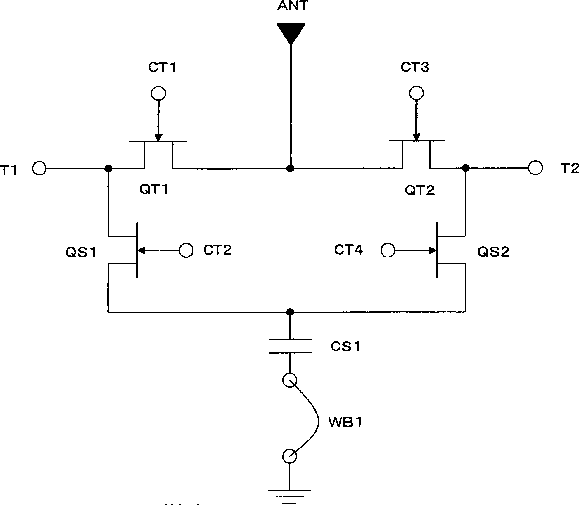
[0048] Figure 6 An equivalent circuit diagram showing an antenna switch circuit in which a shunt capacitor is generalized. exist Figure 6 , the field effect transistors QS1 and QS2 on the shunt side are connected to the upper electrode of the same shunt capacitor CS1, that is, one end. The lower electrode, that is, the other end of the shunt capacitor CS1 is grounded.
[0049] However, taking the capacitance of the shunt capacitor CS1 of the prior art as C and the capacitance of the shunt capacitor CS1 of the present embodiment as C', assuming C=C', the signal input from the high-frequency signal input and output terminal T1 passes through the common shunt capacitor The upper electrode of CS1 leaks to the high-frequency signal input / output terminal T2, and the isolation characteristic becomes worse than that of the prior art. For this reason, it is necessary to change the ground side of the shunt capacitor CS1 to a lower impedance.
[0050] figure 1 It is a circuit dia...
no. 2 example
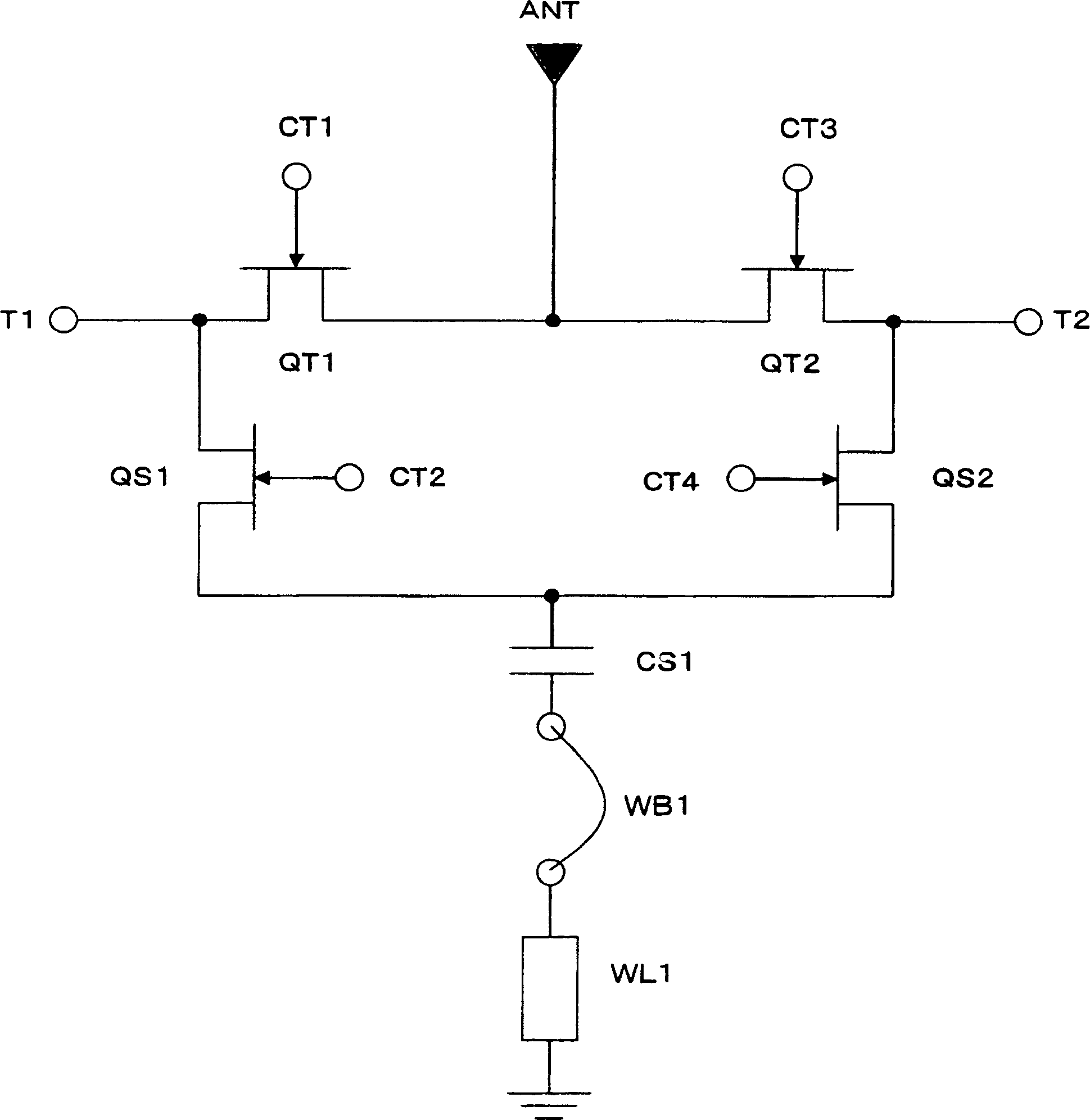
[0061] figure 2 is a circuit diagram showing the configuration of the second embodiment of the antenna switch circuit according to the present invention. exist figure 2 Here, the shunt-side field effect transistors QS1 and QS2 are connected to the upper electrode of the same shunt capacitor CS1, and are grounded through the shunt capacitor CS1, bonding wire WB1, and wiring WL1. Since the bonding wire WB1 and the wiring WL1 are equivalently regarded as an inductor, the shunt capacitor CS1 and the bonding wire WB1 and the wiring WL1 constitute a series resonant circuit.
[0062] In the antenna switch circuit of this embodiment, at least shunt side field effect transistors QS1 and QS2 and through side field effect transistors QT1 and QT2 are formed on a GaAs substrate. The shunt capacitor CS1 may be formed on a GaAs substrate, may be formed inside a laminated substrate (LTCC: Low Temperature Co-fired Ceramics), or may be formed as an external chip component. The wiring WL1 m...
no. 3 example
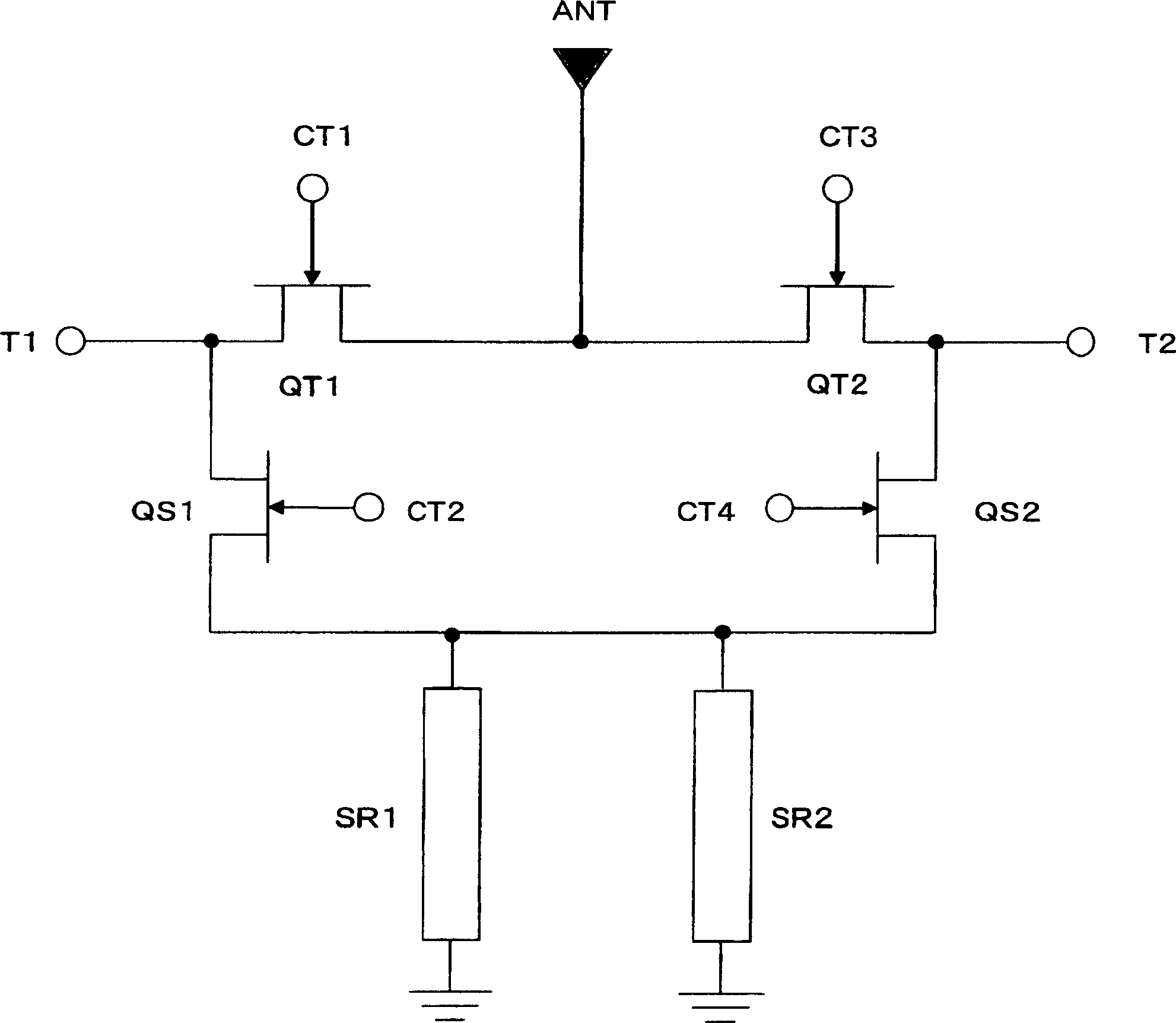
[0074] image 3is a circuit diagram showing the configuration of the third embodiment of the antenna switch circuit according to the present invention. In this embodiment, two series resonant circuits described in the first and second embodiments are provided in parallel. That is, the shunt side field effect transistors QS1, QS2 are grounded through two parallel series resonant circuits SR1, SR2. The attenuation limits of the above two series resonant circuits SR1, SR2 are jointly set to 2 GHz.
[0075] By setting the constants of these two series resonant circuits SR1 and SR2 to the same value, wide-band isolation can be ensured. Thus, for example, high isolation characteristics can be realized by using dual frequencies of the GSM band (900 MHz), the PCS band (1900 MHz), or the DCS band (1800 MHz). That is, by providing two series resonant circuits SR1 and SR2 having the same attenuation limit in parallel, it is possible to widen the limit frequency band and ensure wide-ba...
PUM
 Abstract
Description
Claims
Application Information