Flip ball grid array packaging base plate and making technique thereof

A technology of ball grid array and packaging substrate, which is applied in multilayer circuit manufacturing, semiconductor/solid-state device manufacturing, and printed circuits connected with non-printed electrical components. Low performance and other problems, to achieve the effect of improving electrical performance and reliability, a wide range of options, and affordable prices

Inactive Publication Date: 2005-11-02
美龙翔微电子科技(深圳)有限公司
View PDF0 Cites 53 Cited by
  • Summary
  • Abstract
  • Description
  • Claims
  • Application Information

AI Technical Summary

Problems solved by technology

This process has the disadvantages of difficulty in controlling the alignment of the pressing plate, high process difficulty, low reliability and high cost.

Method used


Image

  • Flip ball grid array packaging base plate and making technique thereof
  • Flip ball grid array packaging base plate and making technique thereof
  • Flip ball grid array packaging base plate and making technique thereof

Examples


Embodiment Construction

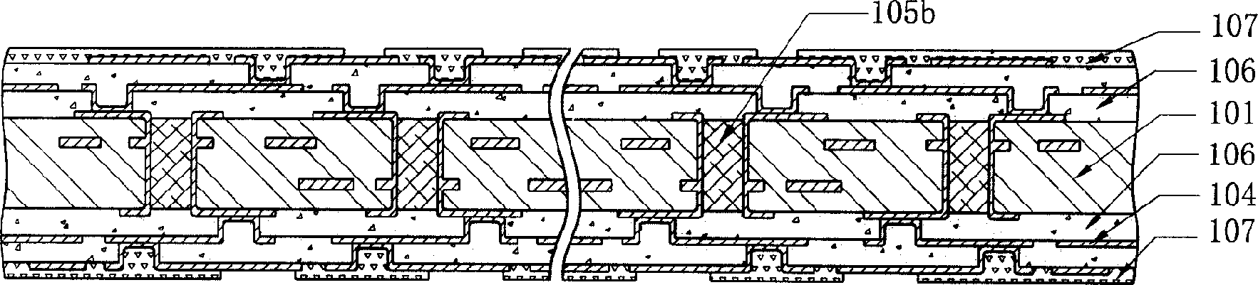
[0028] The manufacturing process of the obtained integrated circuit (IC) FC-BGA package substrate is as follows: 1. Electroplating on the copper plate the metal conductive pillar for the interconnection of the composite multi-metal layer structure

[0029] Such as Figure 7 , 8 As shown, after surface treatment is performed on the reinforced metal copper sheet 201, a photosensitive and anti-electroplating dry film 203 is pasted on the surface of the reinforced metal copper sheet 201. Such as Figure 9-12 As shown, the metal conductive pillars 206 for the interconnection of the composite multi-metal layer structure are formed by the methods of exposure, development, sequential pattern electroplating of Ni204, Au202, Cu205, and film removal.

[0030] 2. After electroplating the metal conductive pillars 206 for the interconnection of the composite multi-metal layer structure on the copper plate, the first application of the insulating dielectric layer and the formation of the circuit ...


PUM


Abstract

The invention discloses a packaging base plate of flip chip ball grid array integrated circuit and the making process. The base plate comprises enhanced metal core layer, insulating medium layer, conductive layer of the ball grid array base plate solder ball connection pattern and the lead pattern anti soldering layer and the back enhancing metal copper plate. Form a hollow in the back enhancing metal copper plate of the base plate and set chips. Coating insulating medium on the enhancing metal copper plate and forming the circuit, getting the final required structure by the special line connection structure and the special process of one-way gradually add layers.

Description

Technical field [0001] The invention relates to an integrated circuit (Integrated Circuit, IC) packaging substrate and its manufacturing process, in particular to a multi-layer packaging substrate circuit that can be directly constructed on a reinforced metal copper sheet by a build-up process (Build Up). Background technique [0002] With the rapid development of electronic technology and the emergence of high-tech electronic products, all kinds of products are designed towards the trend of light, thin, short, and small to provide more convenient use. From the beginning of manufacturing to completion of electronic products, integrated circuit packaging plays an important role, and the packaging form of integrated circuit is divided by the interconnection of substrate and chip. At present, there are two main development directions-wire bonding interconnection ( Bonding) and solder ball interconnection (Solder Bump). At present, two packaging forms coexist, but the development tre...

Claims


Application Information

Patent Timeline
Patent Type & Authority Applications(China)
IPC IPC(8): H01L23/12
Inventor 尤宁圻朱惠贤陈金富兰亦金张烈洋
Owner 美龙翔微电子科技(深圳)有限公司
Why Eureka
Try Eureka