Light beam shaping device in use for semiconductor laser array in high power

A beam shaping, semiconductor technology, applied in semiconductor laser devices, laser devices, optics, etc., can solve the problems of small beam numerical aperture, achieve high numerical aperture, small beam output, high coupling efficiency, simple design and production Effect

Inactive Publication Date: 2005-11-16
CHANGCHUN INST OF OPTICS FINE MECHANICS & PHYSICS CHINESE ACAD OF SCI
View PDF0 Cites 23 Cited by
  • Summary
  • Abstract
  • Description
  • Claims
  • Application Information

AI Technical Summary

Problems solved by technology

The purpose of the present invention is to solve the problem of the output beam quality of the semiconductor laser array on the basis of ensuring high output power and small beam numerical aperture, and simultaneously obtain high power and high quality beam output

Method used


Image

  • Light beam shaping device in use for semiconductor laser array in high power
  • Light beam shaping device in use for semiconductor laser array in high power
  • Light beam shaping device in use for semiconductor laser array in high power

Examples


Embodiment 1

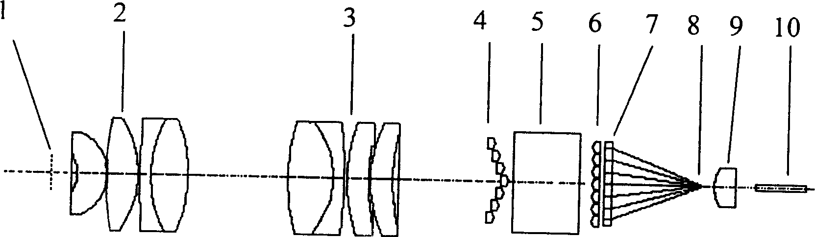
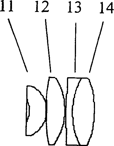
[0014] The first lens group 2 is made up of the first concave-convex lens 11, the first double-convex lens 12, the cemented lens that is the first convex-convex lens 13 and the second double-convex lens 14; 12. The cemented lens is the first concave-convex lens 13 and the second biconvex lens 14. The concave surface of the first concave-convex lens 11 is close to the output end of the laser array 1, and the convex surface of the first concave-convex lens 11 is close to the input surface of the first biconvex lens 12. The output surface of the first lenticular lens 12 is close to the convex surface of the first lenticular lens 13, the concave surface of the first lenticular lens 13 is glued together with the convex input surface of the second lenticular lens 14, and the convex output surface of the second lenticular lens 14 is close to the first lenticular lens 14. The convex input face of the three lenticular lenses 15 .

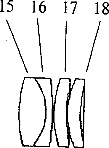
[0015] The second lens group 3 is made up of cemented ...

Embodiment 2

[0021] When the present invention is used in a high-power laser array, the laser array 1 can adopt a laser array of nineteen light-emitting units, each light-emitting unit has a strip width of 150 μm, a period of 500 μm, an area of ​​the light-emitting area of ​​10 mm×0.001 mm, and continuous output at room temperature The optical power is 40W, the divergence angle perpendicular to the p-n junction direction (fast axis) of the laser array is 35°, the numerical aperture is 0.5736, and the divergence angle parallel to the p-n junction direction (slow axis) of the laser array is 7°, the value The aperture is 0.12, and other parameters are the same as in Example 1.


PUM

PropertyMeasurementUnit
divergence angleaaaaaaaaaa

Abstract

A light beam reshaping device consists of laser array, the first lens set, the second lens set, the first planoconvex lens set, quick shaft compression column lens, the second planoconvex lens set, optical fibre array, optical fibre bundle, focusing lens and optical fibre. The device can ensure high coupling rate, high power and high brightness as well as can be used in high power semiconductor laser array.

Description

Technical field: [0001] The invention belongs to the field of semiconductor lasers, and relates to the structural design of a semiconductor laser array beam shaping device. Background technique: [0002] Due to the advantages of small size, light weight, long life and high power, semiconductor laser array has broad application prospects and huge potential market in military, industrial and medical fields, so it has become a research hotspot pursued by countries all over the world. However, due to the inherent structural defects of the semiconductor laser array, the output beam quality of each light-emitting unit is very poor. The specific performance is that the divergence angle of each light-emitting unit in the direction perpendicular to the p-n junction (fast axis) is 30°-40°, parallel to The divergence angle of the p-n junction direction (slow axis) is 7°-10°. Due to the different divergence angles and severe astigmatism in the direction perpendicular to the p-n junctio...

Claims


Application Information

Patent Timeline
Patent Type & Authority Applications(China)
IPC IPC(8): G02B27/09
Inventor 李丽娜史光辉王立军尹红贺刘君
Owner CHANGCHUN INST OF OPTICS FINE MECHANICS & PHYSICS CHINESE ACAD OF SCI
Why Eureka
Try Eureka