Plasma processing apparatus, method for producing reaction vessel for plasma generation, and plasma processing method

A plasma and processing device technology, applied in the field of plasma processing devices, can solve the problems of increased gas operating costs and other issues

Inactive Publication Date: 2005-11-23
MATSUSHITA ELECTRIC WORKS LTD
View PDF0 Cites 31 Cited by
  • Summary
  • Abstract
  • Description
  • Claims
  • Application Information

AI Technical Summary

Problems solved by technology

However, there is much room for improvement considering the supply of plasma or plasma-activated particles to the entire treatment area via a uniform gas flow
In addition, such large-area plasma treatment has another problem that a large consumption of gas leads to an increase in operating costs

Method used


Image

  • Plasma processing apparatus, method for producing reaction vessel for plasma generation, and plasma processing method
  • Plasma processing apparatus, method for producing reaction vessel for plasma generation, and plasma processing method
  • Plasma processing apparatus, method for producing reaction vessel for plasma generation, and plasma processing method

Examples


example 1

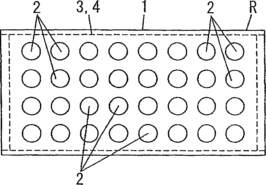
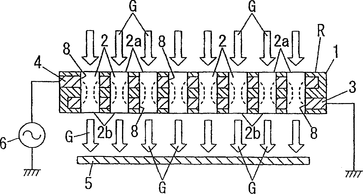
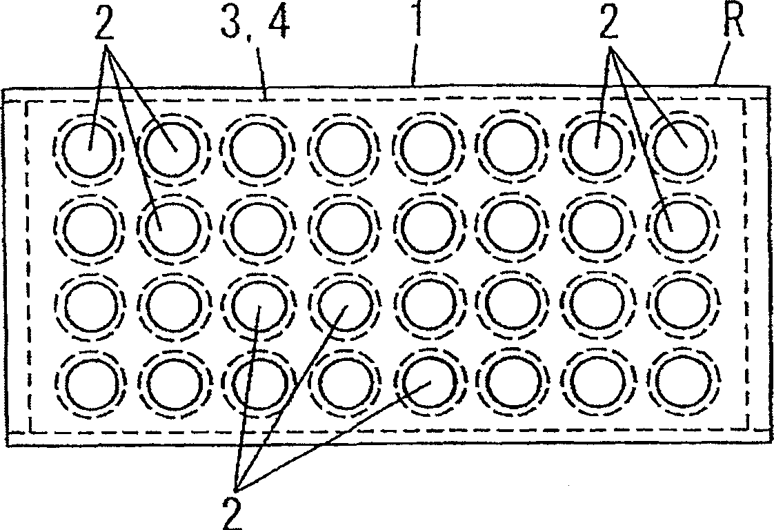
[0125] A conductive film was formed on the surface of the first board (thickness: 0.4 mm) by printing, and then the second board (thickness: 1.4 mm) was placed on the conductive film. Further, a conductive film was formed on the surface of the second board by printing, and then a third board (thickness: 1.4 mm) was placed on the conductive film. In this embodiment, each of the first to third plates is obtained by forming a material containing alumina powder into a plate shape. Each plate has a plurality of apertures, each aperture having a diameter of 1 mm. The plates are placed in layers such that the aperture positions of the individual plates correspond to each other. The conductive film is formed by printing a tungsten layer. A plurality of apertures 8 (each having a diameter of 3 mm, larger than the apertures of the plates) were formed in the conductive film such that each aperture of the plates was placed in each aperture of the conductive film. The stack thus obtaine...

example 2

[0129]A conductive film was formed on the surface of the first board (thickness: 0.7 mm) by printing, and then the second board (thickness: 1.5 mm) was placed on the conductive film. Each of the first and second plates was formed by forming an alumina-containing material into a plate shape, as in the case of Example 1. Each of the first and second plates had a plurality of slit-like apertures each having a width of 1 mm and a length of 22 mm in plan view thereof. The plates are placed in layers such that the positions of the slit-like apertures of the plates correspond to each other. The conductive film was formed by printing a tungsten layer, as in the case of Example 1. In this embodiment, each conductive film is formed in a comb pattern. The stack thus obtained is sintered to obtain a Figure 3A with 3B Reaction vessel R of the structure shown.

[0130] In this embodiment, the insulating member 1 of the reaction container has a thickness of 2.2 mm, and eleven slit-shap...

example 3

[0133] The plasma processing apparatus used in this embodiment is basically the same as that of Example 1, except that the diameters of the pores 8 and the through holes 2 of the electrodes 3, 4 are 1 mm, and the inner surfaces of the pores 8 of the electrodes 3, 4 are exposed to inside of via 2, as Figure 10 shown.


PUM

PropertyMeasurementUnit
diameteraaaaaaaaaa
sizeaaaaaaaaaa
diameteraaaaaaaaaa

Abstract

PROBLEM TO BE SOLVED: To provide a plasma processing apparatus capable of expanding a processing area and of carrying out uniform processing, and allowing design to be easily changed in response to an object of processing.

Description

technical field [0001] The present invention relates to a plasma processing apparatus and method for efficient large-area plasma processing. Background technique [0002] In the past, plasma surface treatment has been widely used for the following purposes: removing impurities such as organic materials from the object to be treated, etching or stripping resists, improving the adhesion of organic films, reducing metal oxides, forming films, electroplating and coating pretreatment, as well as surface modification of various materials and parts. [0003] For example, Japanese Patent Laid-Open [kokai] No. 11-335868 discloses surface treatment using plasma in which plasma is generated by applying a voltage between a pair of electrodes while supplying plasma-generating gas to the discharge space. generated in the discharge space between the electrodes. In this plasma surface treatment, since plasma or plasma activated species (species) is ejected from a single nozzle, and the ob...

Claims


Application Information

Patent Timeline
Patent Type & Authority Applications(China)
IPC IPC(8): B01J19/08
Inventor 柴田哲司山崎圭一田口典幸泽田康志
Owner MATSUSHITA ELECTRIC WORKS LTD
Why Eureka
Try Eureka