Nonvolatile memory unit and its array
A technology of non-volatile storage and charge storage layer, applied in electronic programmable read-only memory, in the field of changing energy barrier height, to achieve the effect of suppressing large resistance effect, suppressing large capacitance effect and solving current waste
- Summary
- Abstract
- Description
- Claims
- Application Information
AI Technical Summary
Problems solved by technology
Method used
Image
Examples
Embodiment 100
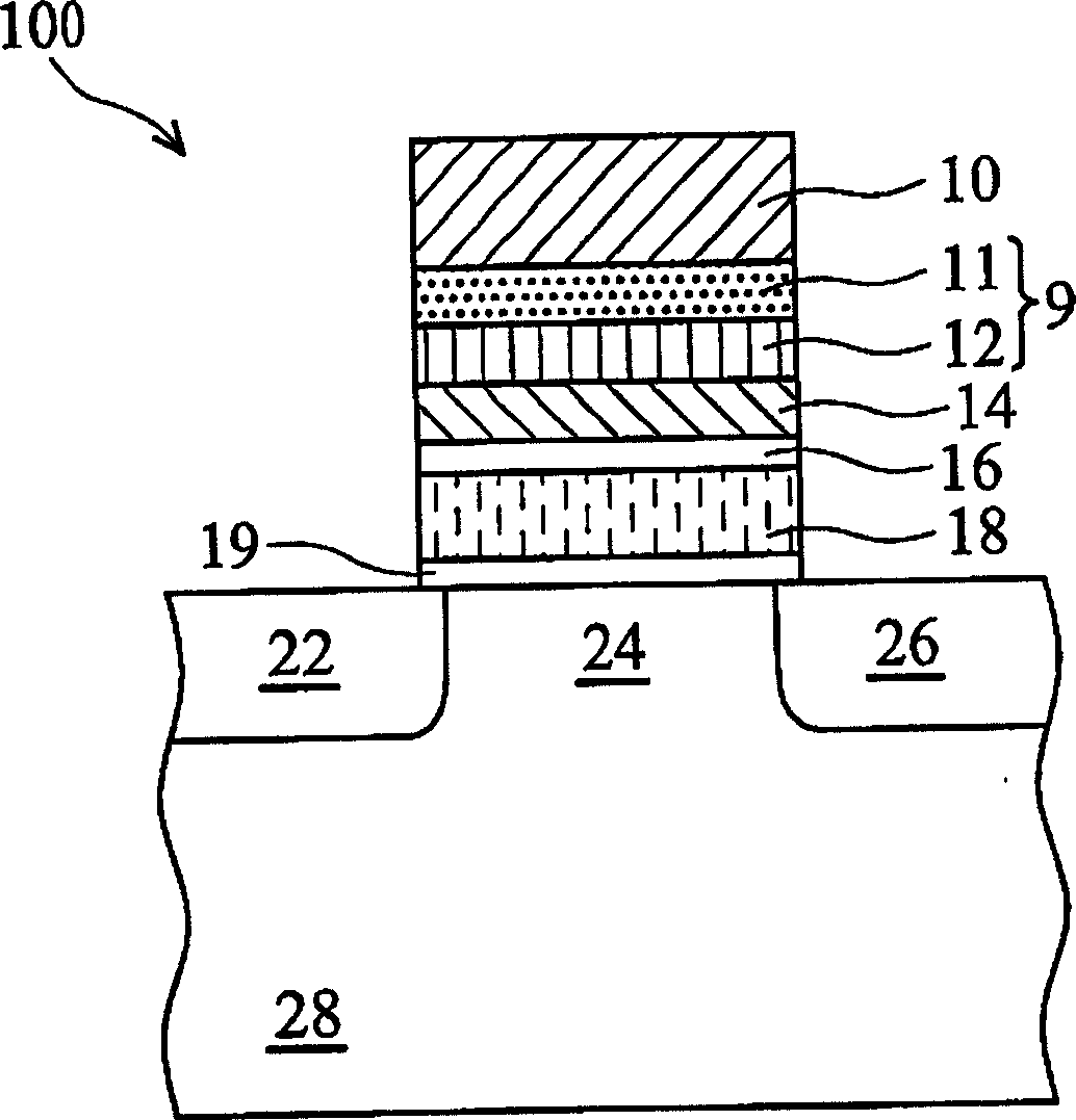
[0077] The symbol N+ used in this specification represents a heavily doped N-type semiconductor material, and the doping concentration of N-type impurities (such as arsenic) contained in it is typically 10 20 (number of atoms / cubic centimeter). The symbol P+ represents a heavily doped P-type semiconductor material, and the doping concentration of P-type impurities (such as boron) contained in it is typically 10 20 (number of atoms / cubic centimeter).
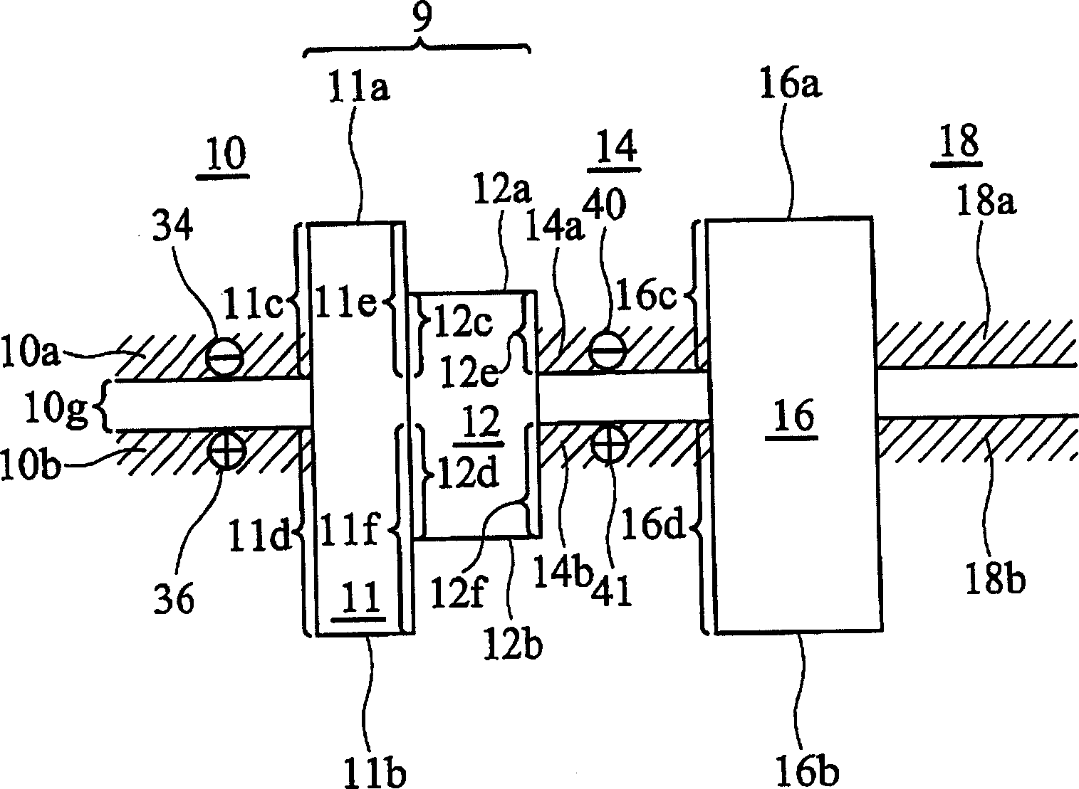
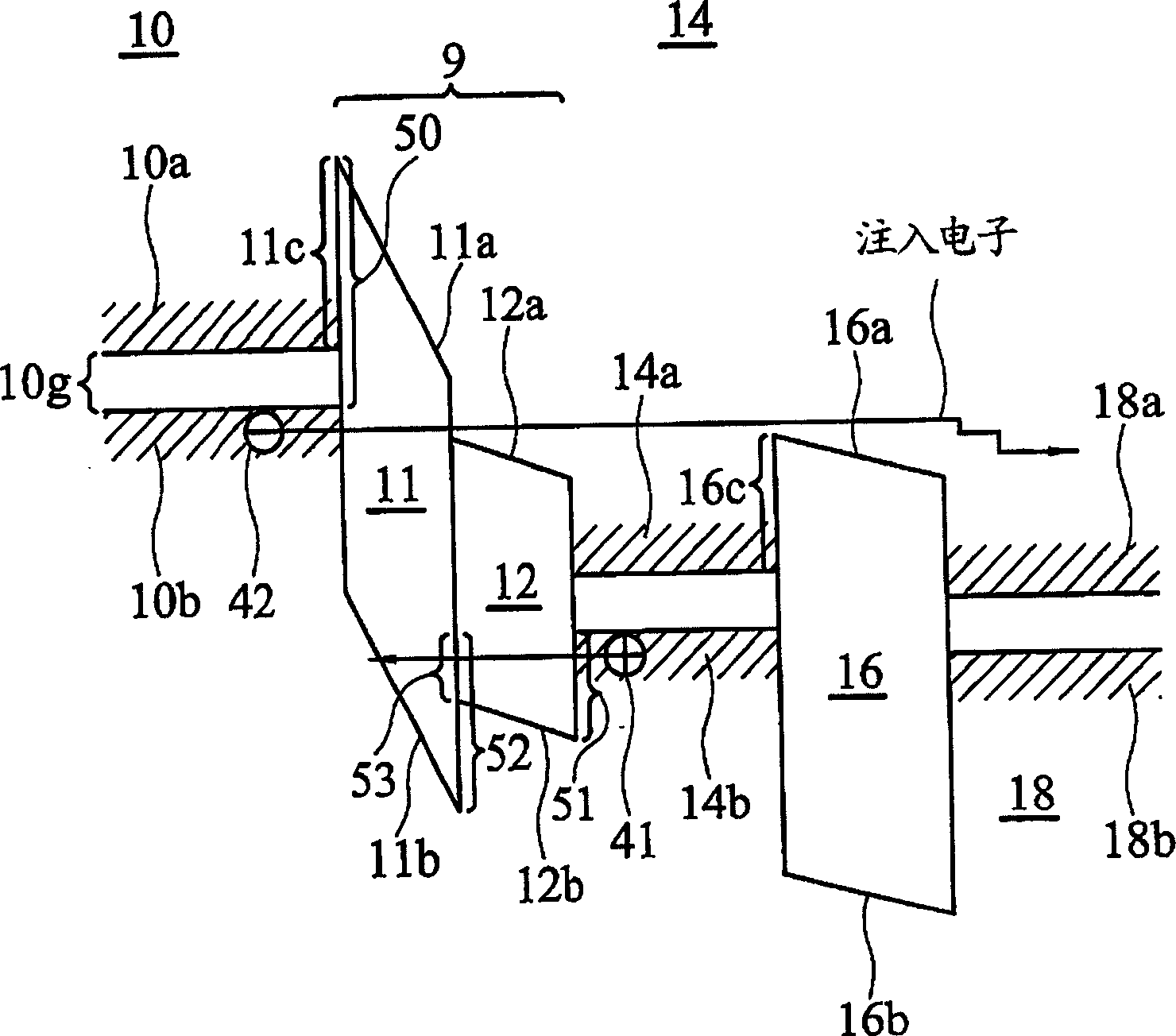
[0078] Figure 1Ais a cross-sectional view showing a cell structure 100 constructed according to an embodiment of the present invention. The figure shows a tunnel gate (hereinafter referred to as TG) 10, a filter 9, a ballistic gate (hereinafter referred to as BG) 14, a floating gate (hereinafter referred to as FG) 18, a source 22, a channel 24, a The drain 26, and a body 28 in a semiconductor substrate (such as a silicon substrate, or a Silicon-On-Insulator substrate). The filter 9 includes a tunneling dielectric (hereinafter...
Embodiment 200
[0192] Figure 11A and Figure 11B The structure of the memory cell 200 according to another embodiment of the present invention and the energy band diagram of the structure under flat energy band conditions are respectively provided. Figure 11A The storage unit 200 of the storage unit 200 is changed to some extent except the part between TG 10 and BG 14 in the filter 9, and the rest are all the same as Figure 1A The structures presented are similar. These changes will be described below. refer to Figure 11A , which shows that the filter 9 includes an upper tunneling dielectric 71 (hereinafter referred to as UTD), a lower tunneling dielectric 72 (hereinafter referred to as LTD), and a barrier material 73 disposed between the UTD 71 and the LTD 72 (hereinafter referred to as BM). UTD 71 may be an oxide or other type of dielectric material, such as the material considered TD 11 within cell 100 . LTD 72 may be a dielectric material with a lower energy gap than UTD 71 and ...
Embodiment 300
[0198] Figure 12A In addition to will Figure 11A The BM 73 is replaced by a plurality of barrier nanocrystals (hereinafter referred to as BNC) 74, and the rest are the same as Figure 11A Similar unit structures are similar, and the energy gaps of multiple BNCs 74 in the figure are similar to or larger than those of TG 10 . BNC 74 may be spherical with a diameter approximately the wavelength of charge carriers such as electrons or holes. Typically, BNC 74 has a diameter of about 30 Angstroms to about 200 Angstroms. The barrier nanocrystals 74 can be fabricated by using Ultra-High Vacuum Chemical-Vapor-Deposition (UHVCVD) technology well known in the art. The blocking nanocrystal 74 is used as an "island" between the TG 10 and the BG 14 to allow charge carriers to hop across it. Specifically, when a proper bias voltage is applied between the TG 10 and the BG 14 , charge carriers in the TG 10 will be emitted to the BNC 74 through a tunneling mechanism, and then tunnel into...
PUM
 Abstract
Description
Claims
Application Information


