A planar inductive component and an integrated circuit comprising a planar inductive component

A planar inductor and component technology, applied in electrical components, transformer/inductor components, circuits, etc., can solve problems such as low quality factor, achieve high quality factor, and improve efficiency.

Inactive Publication Date: 2006-01-18
NXP BV
View PDF1 Cites 23 Cited by
  • Summary
  • Abstract
  • Description
  • Claims
  • Application Information

AI Technical Summary

Problems solved by technology

A still existing disadvantage of the known planar in

Method used


Image

  • A planar inductive component and an integrated circuit comprising a planar inductive component
  • A planar inductive component and an integrated circuit comprising a planar inductive component
  • A planar inductive component and an integrated circuit comprising a planar inductive component

Examples


Embodiment Construction

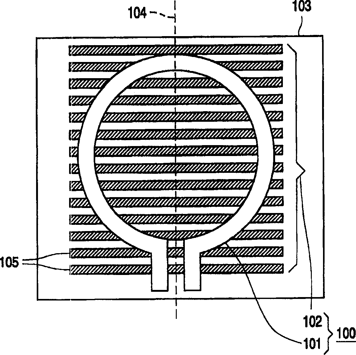
[0033] figure 1 A top view of an embodiment of a planar inductive element according to the invention is shown. The illustrated planar inductive element 100 includes a coil 101 and a patterned ground shield 102 . The planar inductive element 100 is located on top of another layer, the substrate 103 . The coil 101 is essentially a track of conductive material, such as aluminium, that forms a generally circular ring. The trajectory is symmetrical about a mirror plane 104 whose direction is perpendicular to the surface of the substrate 103 . A patterned ground wire shield is located between the coil 101 and the substrate 103 . The ground shield 102 includes a plurality of traces 105 formed from a conductive material, such as aluminum or polysilicon. The trace 105 lies in a plane parallel to the surface of the substrate, and the direction of the trace 105 is perpendicular to the mirror plane 104 .

[0034] At the terminals of the planar inductive element 100, the voltage diffe...


PUM


Abstract

The invention relates to a planar inductive component arranged over a substrate ( 103 ). The substrate in a first plane, a patterned ground shield ( 102 ), for shielding the winding ( 101 ) from the substrate ( 103 ). The winding ( 101 ) is at least substantially symmetrical plane. The patterned ground shield ( 102 ) comprises a plurality of electrical conductive first tracks ( 105 ) situated in a first ground shield plane in parallel with the first plane. The first tracks have an orientation perpendicular to the mirror plane ( 104 ). Without the patterned ground shield ( 102 ) the winding ( 101 ) is capacitively coupled to the substrate ( 103 ). The substrate resistance results in a degradation of the quality factor of the inductive component ( 100 ). The patterned ground shield ( 102 ) shields the winding ( 101 ) from the substrate ( 103 ), thereby eliminating the degrading effect of the substrate. To prevent a reduction in the effective self inductance of the planar inductive component loop currents have to be prevented in the patterned ground shield, while at the same time transfer of charges induced in the mirrored halves of the winding ( 100 ) have to be facilitated. This is achieved by the first tracks ( 105 ).

Description

technical field [0001] The present invention relates to a planar inductive element comprising: [0002] - a coil lying in the first plane, [0003] - Patterned ground shield for shielding the coil from other layers. [0004] The invention also relates to an integrated circuit comprising a substrate and a planar inductive element. Background technique [0005] Such a planar inductive element is disclosed in International Patent Application Serial No. WO98 / 50956. Such planar power components are widely used, for example, in integrated circuits operating at RF frequencies. For example, such circuits will find application in wireless communication devices such as cellular telephones and wireless LAN base stations. [0006] The disclosed planar inductive element is part of an integrated circuit. The patterned ground shield of the planar inductive element is located between its coil and the semiconductor substrate on which the planar inductive element is formed. The disclose...

Claims


Application Information

Patent Timeline
IPC IPC(8): H01F17/00H01L23/522H01F27/34H01F27/36
CPCH01L2924/0002H01L23/5227H01F17/0013H01F2017/008H01F17/0006H01F27/34H01F27/367H01F2021/125H01F27/36H01F27/363H01L2924/00H01L27/04H01L29/00
Inventor L·F·蒂梅杰R·J·哈文斯D·M·W·里纳尔特斯N·帕洛维克H·韦恩斯特拉E·范德海登
Owner NXP BV
Why Eureka
Try Eureka