

Plasma generation device, plasma control method, and substrate manufacturing method
A plasma and generation device technology, which is applied in the fields of plasma, semiconductor/solid-state device manufacturing, and the method of chemically changing substances by using atmospheric pressure, which can solve problems such as damage to plasma uniformity
- Summary
- Abstract
- Description
- Claims
- Application Information
AI Technical Summary
Problems solved by technology
Method used
Image

Examples
no. 1 Embodiment
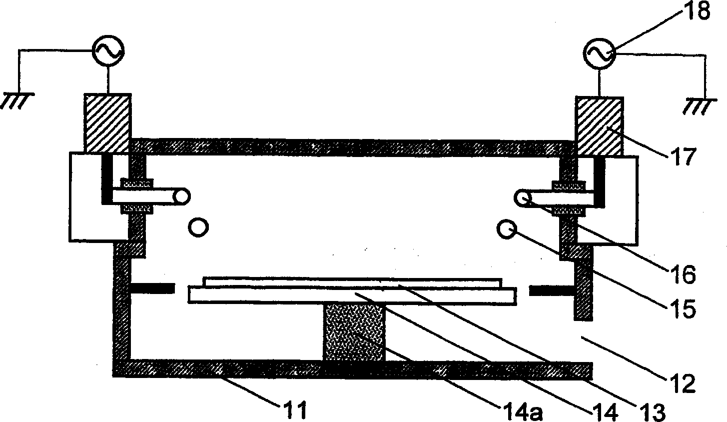
[0076] Respectively figure 1 shows a cross-sectional view in the vertical direction of the first embodiment of the plasma generation device of the present invention, in figure 2 shows a side view of the device, the image 3 A plan view of the device is shown in .
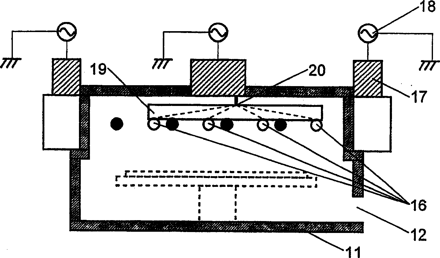
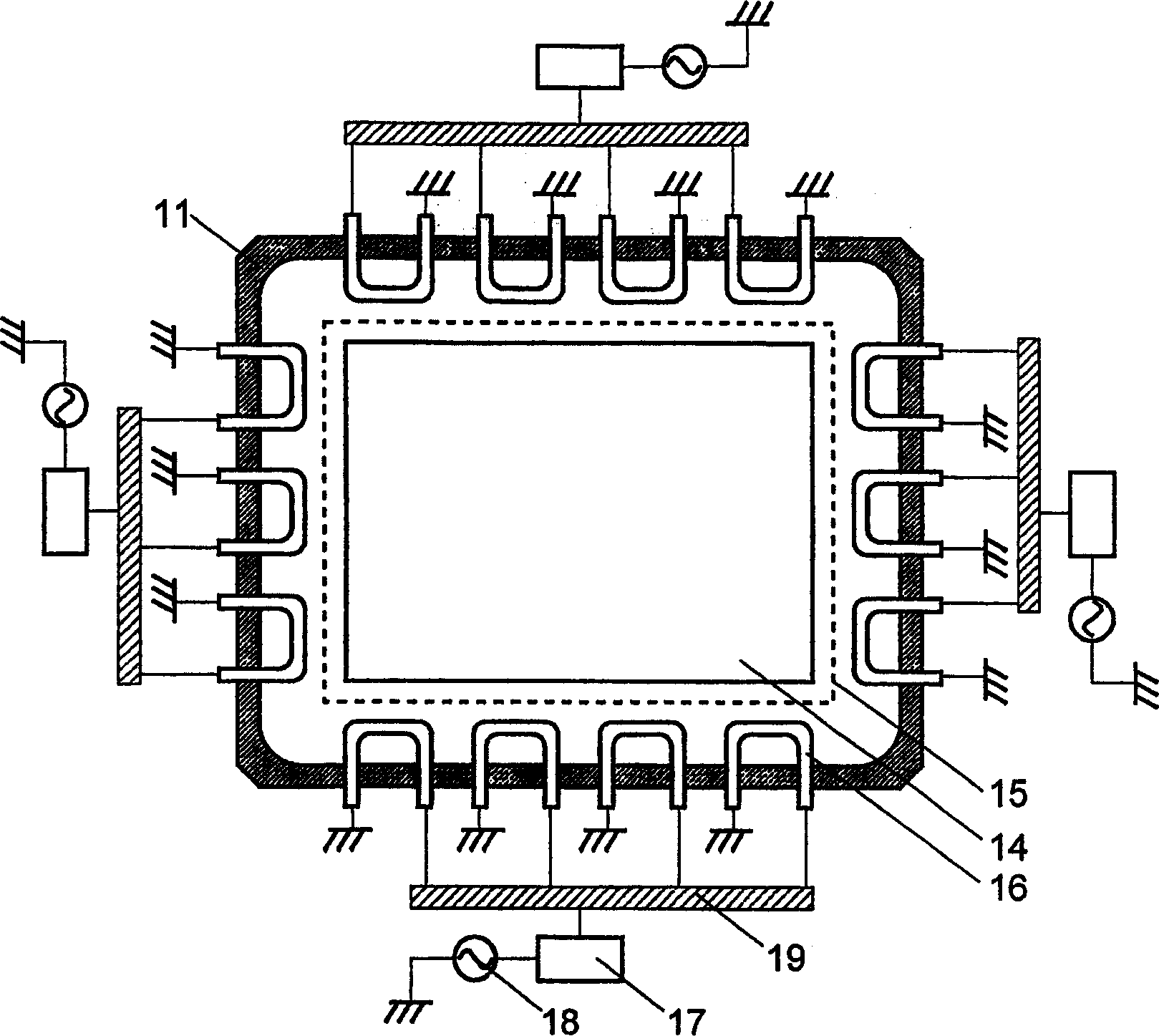
[0077] The inside of the vacuum vessel 11 constitutes a plasma generation chamber of the plasma generation device. Vacuum container 11 inside such as image 3 As shown, the planar shape is a rectangle (rectangle), the length of its long side is 130mm, and the length of its short side is 100mm. A vacuum pump (not shown) is connected to the vacuum container 11 to maintain the inside of the vacuum container 11 at a predetermined vacuum degree. A rectangular planar substrate table 14 with a long side of 94 cm and a short side of 76 cm for loading a substrate 13 to be processed is provided in the vacuum container 11 . The substrate table 14 can be raised and lowered by a lifting unit 14a provided at the lower part ...
no. 2 Embodiment
[0092] In the second embodiment, the configuration of the plasma generation device focusing on the aspect ratio of the antenna will be described.
[0093] Figure 10 A plan view of the second embodiment is shown in . In this plasma generation device, only the aspect ratio of the antenna 26 in the device configuration of the first embodiment is changed. Thus, in Figure 10 In, the same constituent elements as those of the first embodiment are added with image 3 same symbol. The number of high-frequency power sources and the number of antennas connected to each high-frequency power source are also the same as those in the first embodiment. In the device shown in this figure, if Figure 11 As shown in (a), the aspect ratio of all the antennas 26 is set to 2 (vertical:horizontal=2:1). Additionally, if Figure 11 As shown in (b), the aspect ratio of the antenna 16 of the first embodiment is 1 (vertical:horizontal=1:1). The area S of the conductor-enclosed region of the ant...
no. 3 Embodiment
[0101] In the third embodiment, the configuration of the plasma generation device focusing on the polarities of adjacent electrodes of adjacent antennas will be described.
[0102] Figure 16 A plan view of the third embodiment is shown in . Adding and image 3 same symbol. The number of high-frequency power sources and the number of antennas connected to each high-frequency power source are the same as those in the first embodiment. In this plasma generating apparatus, only the electrode polarities of the high-frequency antennas 16 in the apparatus configuration of the first embodiment are changed. Specifically, in an antenna group composed of three or four antennas installed on the same side wall, adjacent electrodes of adjacent high-frequency antennas are set to have the same polarity. For example, in the antenna group 31a, the electrodes on the adjacent sides of the adjacent high-frequency antenna 16a and high-frequency antenna 16b are all connected to the impedance in...
PUM
| Property | Measurement | Unit |
|---|---|---|
| Length | aaaaa | aaaaa |
Abstract
Description
Claims
Application Information