Check patentability & draft patents in minutes with Patsnap Eureka AI!

Improved method for reading a non-volatile memory cell adjacent to an inactive region of a non-volatile memory cell array

A non-volatile storage and storage cell technology, applied in the field of flash memory cell devices, can solve the problems of lowering the threshold voltage of the storage cell, depletion of the charge storage area, etc.

Active Publication Date: 2006-03-08
CYPRESS SEMICON CORP
View PDF0 Cites 2 Cited by
  • Summary
  • Abstract
  • Description
  • Claims
  • Application Information

AI Technical Summary

Problems solved by technology

Multiple consecutive erase cycles cause depletion of the charge storage region, thereby lowering the threshold voltage of the memory cell, even in its erased (unprogrammed) state

Method used


Image

  • Improved method for reading a non-volatile memory cell adjacent to an inactive region of a non-volatile memory cell array
  • Improved method for reading a non-volatile memory cell adjacent to an inactive region of a non-volatile memory cell array
  • Improved method for reading a non-volatile memory cell adjacent to an inactive region of a non-volatile memory cell array

Examples


Embodiment Construction

[0039] The present invention will now be described in detail with reference to the accompanying drawings. In the drawings, the same reference numerals are used to designate the same components. Moreover, the drawings are not drawn to scale, and the dimensions of some features are intentionally drawn larger for clarity.

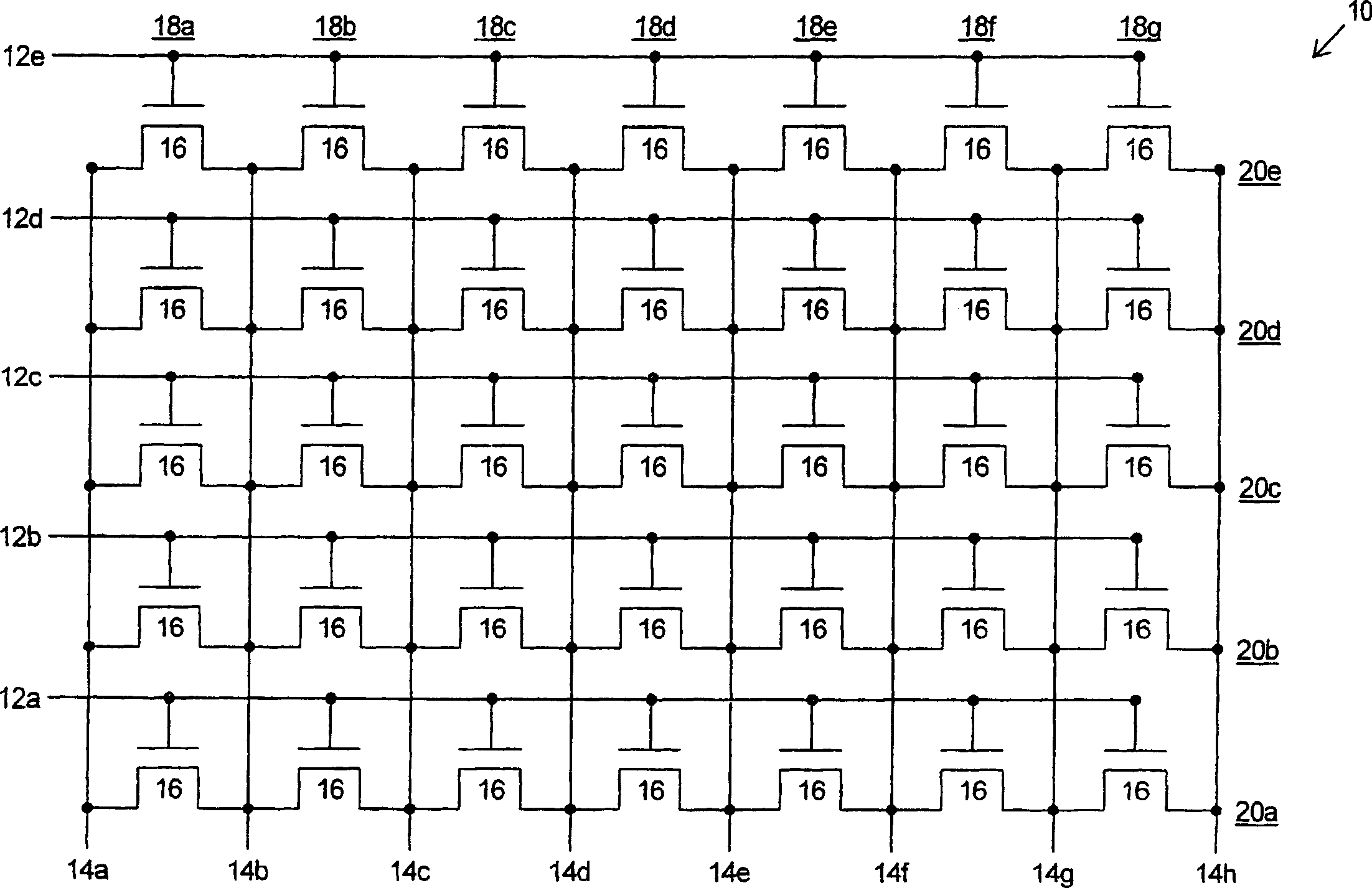
[0040] figure 2 An example embodiment of a non-volatile charge trapping dielectric flash memory cell system 30 is shown in block diagram form. System 30 includes array 40 of non-volatile charge trapping memory cells 48 fabricated on a crystalline semiconductor substrate and array control circuitry 62 .

[0041] The array 40 of non-volatile charge trapping dielectric flash memory cells 48 is arranged in a matrix format, the memory cells 48 being arranged in vertical columns 45a to 45h and orthogonal horizontal rows 43a to 43h. Each memory cell 48 in a column 45 shares the same channel region and two bit line diffusion regions 49 with another memory cell 48 i...


PUM


Abstract

A method of storing a data pattern and reproducing the data pattern within an array 30 of memory cells 48, which includes active columns 45b and 45g and inactive columns 46c and 45f, comprises storing the data pattern within the active columns 45b and 45g. An inactive memory cell programming pattern 32 is identified. The inactive memory cell programming pattern 32 identifies all, or a selected plurality, of the memory cells 48 in the inactive columns 45c and 45f in which a charge is to be stored for the purpose of periodically storing a charge in such memory cells 48 to prevent over erasure, during bulk erase, and leakage to active memory cells 48.

Description

technical field [0001] The present invention relates generally to flash memory cell devices, and more particularly to improvements in systems and methods for reading charge previously stored in a column of charge trapping dielectric flash memory cells adjacent to a passive column. Background technique [0002] The traditional floating gate flash memory type electrically erasable programmable read-only memory (EEPROM) uses a memory cell (memory cell), which is characterized in that it is located on a crystalline silicon substrate and has a tunnel oxide (SiO 2 ), a polysilicon floating gate on the tunnel oxide, an interlayer dielectric (typically an oxide, nitride, or oxide stack) on the floating gate, and a control gate on the interlayer dielectric vertical stack. Within the substrate are a channel region underlying the vertical stack, and source and drain diffusion regions at opposite ends of the channel region. [0003] Floating gate flash memory cells are programmed by i...

Claims


Application Information

Patent Timeline
IPC IPC(8): G11C29/00G11C16/34G11C16/04
CPCG11C29/82G11C16/0491G11C16/3404G11C16/00G11C29/00
Inventor E·夏D·G·汉密尔顿M-H·谢E·朗宁E·阿吉明陈伯伶M·W·伦道夫何毅
Owner CYPRESS SEMICON CORP
Features
  • R&D
  • Intellectual Property
  • Life Sciences
  • Materials
  • Tech Scout
  • Unparalleled Data Quality
  • Higher Quality Content
  • 60% Fewer Hallucinations
Learn More