

Microlens array, method of fabricating microlens array, and liquid crystal display apparatus with microlens array
A technology of liquid crystal display device and microlens array, which is applied to photolithography process exposure devices, lenses, microlithography exposure equipment, etc., can solve problems such as increased cost and reduced production efficiency, and achieves excellent production efficiency and easy optical axis. alignment effect
- Summary
- Abstract
- Description
- Claims
- Application Information
AI Technical Summary
Problems solved by technology
Method used
Image

Examples
Embodiment 1
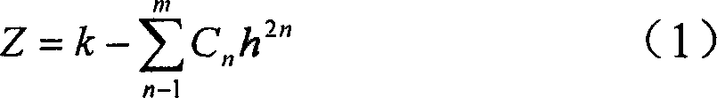
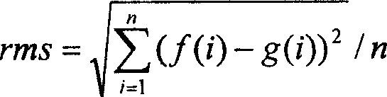
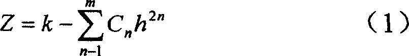
[0083] In this embodiment, the inventors found that the thickness of the transparent substrate on the backlight side of the liquid crystal panel included in the transflective liquid crystal display device and the radiation component of the backlight incident from the backlight to the liquid crystal panel greatly affect the performance of the liquid crystal display device. Display brightness. Furthermore, the relationship between the aperture diameter and the emission luminance in order to obtain sufficient external light was clarified. The present invention improves the display brightness of a transflective liquid crystal display device by specifying them.
[0084]First, the arrangement of the microlens array in the liquid crystal display device and the optical effect of the microlens will be described. FIG. 1 is a cross-sectional view showing a liquid crystal display device of this embodiment. The liquid crystal display device of Example 1 of the present invention is a so-c...
Embodiment 2
[0099] In this example, the method of manufacturing the microlens array and the liquid crystal display device having the microlens array described in Example 1 will be described. In addition, the same code|symbol as Example 1 shows the same or equivalent part as Example 1, and the description is abbreviate|omitted.
[0100] The manufacturing process of the microlens array of this embodiment is divided into the following steps. That is, laser writing is used to write the mask pattern on the dry plate to make the first step of the master grayscale mask, and to expose the photosensitive emulsion base plate through the master grayscale mask to make the second step of the master grayscale mask , form exposure micro-lenses on the master grayscale mask to form the third process of the master grayscale mask with lenses, and then pass the master grayscale mask with lenses to the photosensitive material coated on the transparent substrate 102 Exposure of the permanent resin layer, the ...
Embodiment 3
[0186] This embodiment is a modified example of the first and second steps of the second embodiment. In the second embodiment, a method of forming the convex microlens 202 on the transparent substrate 102 was described, but in this embodiment, an example of forming the concave microlens 202 on the transparent substrate 102 will be described.
[0187] In this embodiment, a grayscale mask having a transmittance pattern opposite to that of the grayscale mask 400 used in Embodiment 2 above is used. That is, the transmittance is highest at the outer periphery of the lens forming region 401a, the light transmittance changes concentrically in the lens forming region 401a, and the light transmittance is lowest at the center of the lens forming region 401a.
[0188] In this embodiment, the light transmittance of the region (referred to as the transmission region 401c) corresponding to the light-shielding region 401b in FIG. The outer circumference decreases concentrically toward the c...
PUM
| Property | Measurement | Unit |
|---|---|---|
| Diameter | aaaaa | aaaaa |
| Area | aaaaa | aaaaa |
| Thickness | aaaaa | aaaaa |
Abstract
Description
Claims
Application Information