Physical interface of NAND gate quick flashing storage, interface method and management equipment

A non-gate flash and physical interface technology, applied in the field of interface equipment, can solve problems such as high CPU consumption, high power consumption, and compatibility difficulties, and achieve the effect of saving resources and reducing costs

Inactive Publication Date: 2006-03-29
VIMICRO CORP
View PDF0 Cites 2 Cited by
  • Summary
  • Abstract
  • Description
  • Claims
  • Application Information

AI Technical Summary

Problems solved by technology

[0004] The physical interface of the prior art has the following problems: 1) CPU consumption is relatively high
Since the entire read and write sequence is actually generated by the firmware function, and the CPU needs several clock cycles to execute an assembly instruction, the CPU must work at a frequency several times higher than that of the flash memory read and write interface, which is not conducive to using low-end to reduce costs; 2) High main frequency will cause higher power consumption; 3) Managing the entire timing operation will take up a lot of resources; 4) Using firmware to manage interface timing makes it difficult to be compatible with various flash memories; 5) In addition, due to different The read and write speeds of the flash memory interfaces are quite different, and it is difficult for the physical interface of the existing technology to give full play to the best speed of different flash memories

Method used


Image

  • Physical interface of NAND gate quick flashing storage, interface method and management equipment
  • Physical interface of NAND gate quick flashing storage, interface method and management equipment
  • Physical interface of NAND gate quick flashing storage, interface method and management equipment

Examples


Embodiment Construction

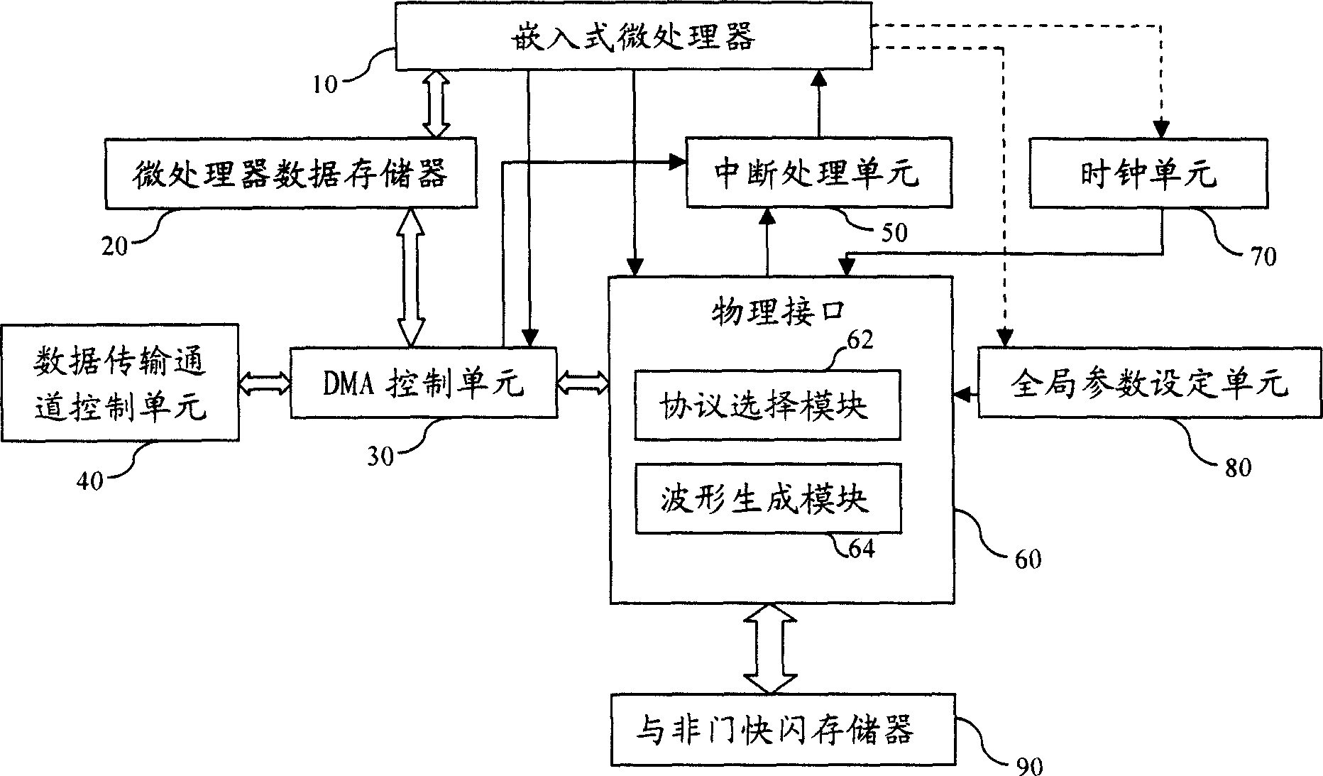
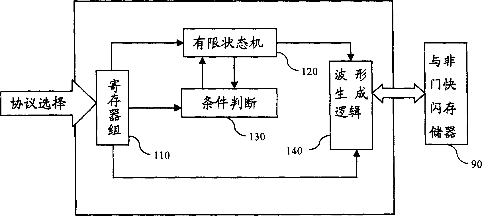
[0018] figure 1 is a schematic diagram of a flash memory management device according to an embodiment of the present invention. exist figure 1 Among them, the flash memory management device includes an embedded microprocessor 10, a microprocessor data memory 20, a direct memory access (referred to as DMA) control unit 30, a data transmission channel control unit 40, an interrupt processing unit 50, a physical interface unit 60, a clock unit 70, and a global parameter setting unit 80. The flash memory management device is used to connect to a NAND flash memory (abbreviated as flash memory) 90 and perform management operations on it. The management operations include read, write, copyback read (Copybackread), copyback write (Copybackwrite), and erase (Erase).

[0019] The embedded microprocessor 10 manages the behavior of the flash memory 90 , and its operations on the flash memory are completed by the physical interface unit 60 . When the embedded microprocessor 10 needs to...


PUM


Abstract

The present invention provides a physical interface for NAND gate flash memory, interface method and management equipment. Said physical interface includes protocol selection unit for selecting correspondent protocol according to global parameter of NAND gate flash memory and waveform generation unit for producing waveform required for operating NAND gate flash memory based on external clock according to the protocol selected by protocol selection unit. Besides, said invention also provides several obvious advantages of said interface, method and management equipment.

Description

field of invention [0001] The present invention relates to an interface device, in particular to a physical interface provided for a NAND flash memory; The physical interface, the interface method and the management device for the NAND flash memory are provided for the interface between the flash memories. Background technique [0002] NAND flash memory (hereinafter referred to as flash memory) does not have a storage controller itself, and its structure can be regarded as composed of many small blocks, each of which can store a certain amount of information, similar to clusters of a hard disk. The reading and writing of the flash memory is also carried out in units of blocks and pages, using, for example, 8-bit I / O ports to access data. Flash memory has a large capacity, low cost, and can achieve a relatively high speed, so it is widely used. The basic working method of flash memory is to read sequentially. One block is written or read and then the next one is followed. I...

Claims


Application Information

Patent Timeline
Patent Type & Authority Applications(China)
IPC IPC(8): G06F3/06
CPCG06F13/1694G11C16/20
Inventor 张浩史大北
Owner VIMICRO CORP
Why Eureka
Try Eureka