
Automatic tracking monitoring system for products processing catalog of semiconductor manufacturing factory

An automatic tracking and manufacturing plant technology, applied in the field of automation systems, can solve the problems of not being able to reasonably formulate the processing time sequence, not being able to organize production most effectively, and not being able to track and monitor online processing status in real time

Inactive Publication Date: 2006-05-17
SEMICON MFG INT (SHANGHAI) CORP +1
View PDF0 Cites 14 Cited by
  • Summary
  • Abstract
  • Description
  • Claims
  • Application Information

AI Technical Summary

Problems solved by technology

[0007] In order to overcome the above-mentioned product planners in semiconductor device manufacturing plants, customer service personnel and sales personnel cannot track and monitor the online processing status of customer products on the production line in real time, and cannot fully understand and digest the working status information of each related machine. The present invention is proposed based on shortcomings such as working out the processing time sequence of various product workpieces in each relevant machine platform, not being able to organize production most effectively, and delivering goods to customers on schedule and with high quality.

Method used


Image

  • Automatic tracking monitoring system for products processing catalog of semiconductor manufacturing factory

Examples


Embodiment Construction

[0019] Below in conjunction with accompanying drawing, describe in detail the operation of the automatic tracking and monitoring system for the customer's product processing catalog of the semiconductor manufacturing plant according to the present invention. In this way, the automatic tracking and monitoring system for the customer product processing catalog of the semiconductor manufacturing plant according to the present invention is illustrated.

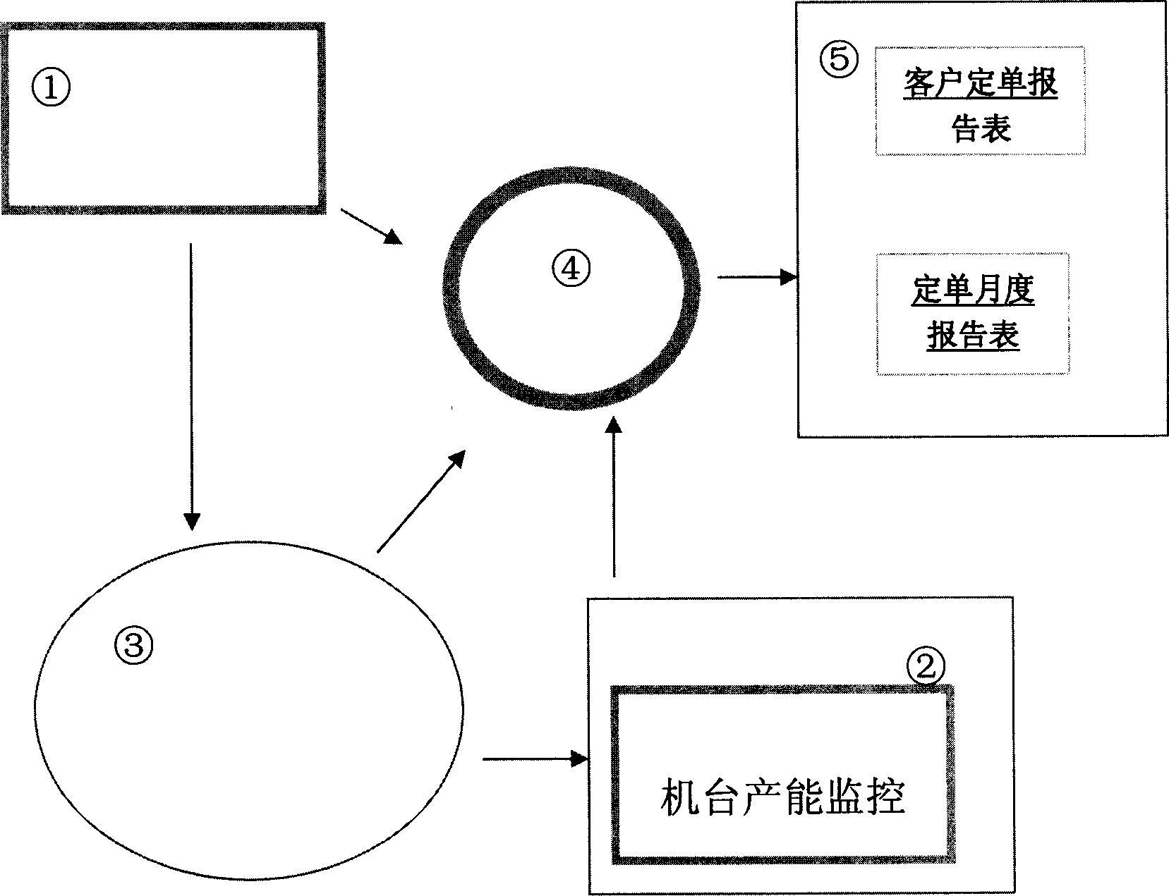
[0020] The operation of the system includes the following steps: Step 1, the customer-based product manufacturing information storage device ① stores data such as the catalog of customer products to be produced, the types and quantities of various products to be produced, and the delivery dates of various products, Input these data into the capacity monitoring device ② of each machine in the production line and the customer's production dispatching center ④ through the company's LAN; Step 2, the capacity monitoring device ② of each...


PUM


Abstract

An automatic tracking and monitoring system of client product processing catalog in semiconductor manufacturer comprises storage unit of product processing information by using client as unit, device for monitoring capacity of each machine set on production line, tracking and monitoring unit of client product processing catalog, producing and dispatching centre of client product, predicting and issuing unit of client product delivery information.

Description

technical field [0001] The invention relates to an automation system for a semiconductor device manufacturing factory, in particular to an automatic tracking and monitoring system for a product processing catalog of a semiconductor device manufacturing factory. Background technique [0002] Generally speaking, in the current semiconductor manufacturing industry, in order to improve production efficiency and reduce production costs, the design unit and manufacturing unit of semiconductor devices are separated, that is to say, the design unit of semiconductor devices specializes in the circuit and structure design of semiconductor devices , while the semiconductor device manufacturing unit specializes in manufacturing semiconductor devices according to the circuit and structure of the semiconductor device designed by the semiconductor device design unit. [0003] Therefore, semiconductor device manufacturers produce a wide variety of semiconductor devices in different quantiti...

Claims


Application Information

Patent Timeline
Patent Type & Authority Applications(China)
IPC IPC(8): H01L21/00G06Q90/00
Inventor 俞晓华向玉坤施南全刘慧甄彭久晏陈鼎崴
Owner SEMICON MFG INT (SHANGHAI) CORP
Learn More