Laminated mould of multi-layer circuit board

A technology of circuit boards and molds, applied in multilayer circuit manufacturing, printed circuit, printed circuit manufacturing, etc., can solve the problems of affecting lamination speed, high manufacturing cost of positioning system, and inability to reuse

Inactive Publication Date: 2006-05-31
李小元
View PDF0 Cites 18 Cited by
  • Summary
  • Abstract
  • Description
  • Claims
  • Application Information

AI Technical Summary

Problems solved by technology

The disadvantages of this laminated mold are:
[0005] 1. The production cost of the positioning system of the entire multilayer circuit board is relatively high. During the lamination process of each multilayer circuit board, the release film 8 and the aluminum plate 7 must be used, and the release film 8 and the aluminum plate 7 can only be used once Permanent use, can not be reused, not only the process is complicated, but also the cost is high
[0006] 2. The upper template 1 and the lower template 2 of the mold are too thick, the mold is heavy, not only the heat transfer speed is slow, but also the heat transfer is uneven, which affects

Method used


Image

  • Laminated mould of multi-layer circuit board
  • Laminated mould of multi-layer circuit board
  • Laminated mould of multi-layer circuit board

Examples


Embodiment Construction

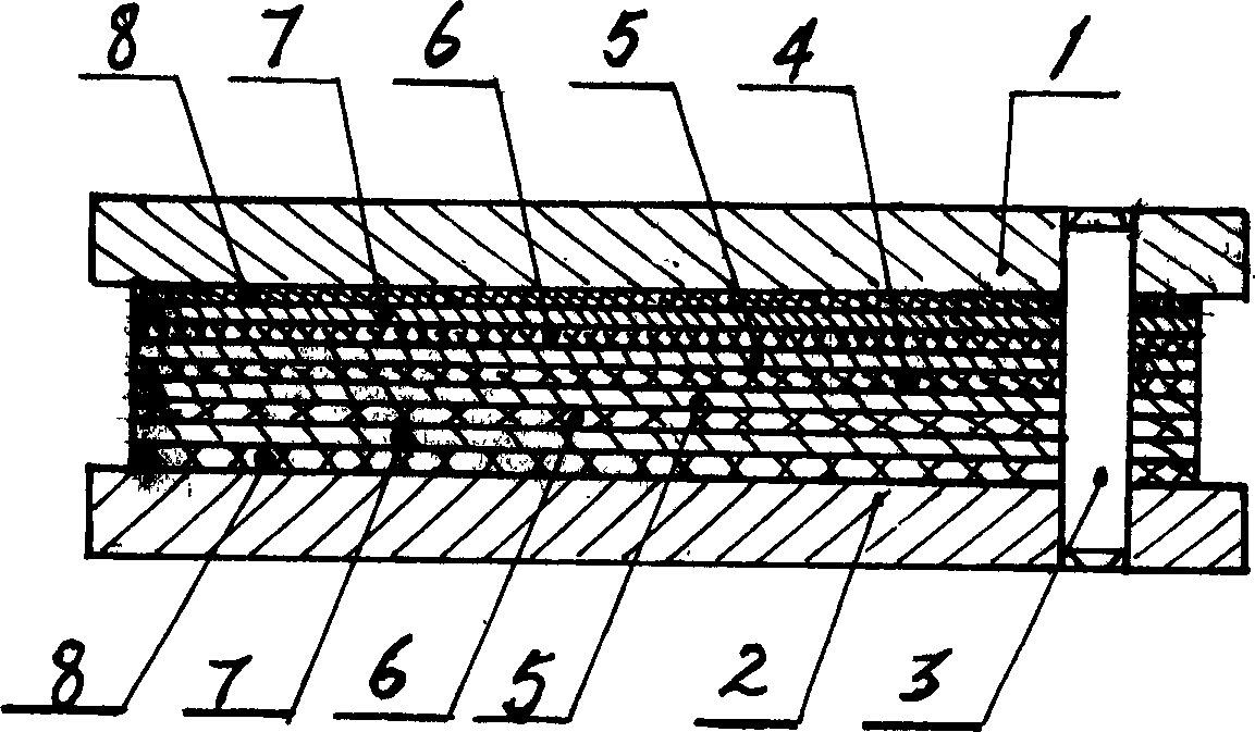
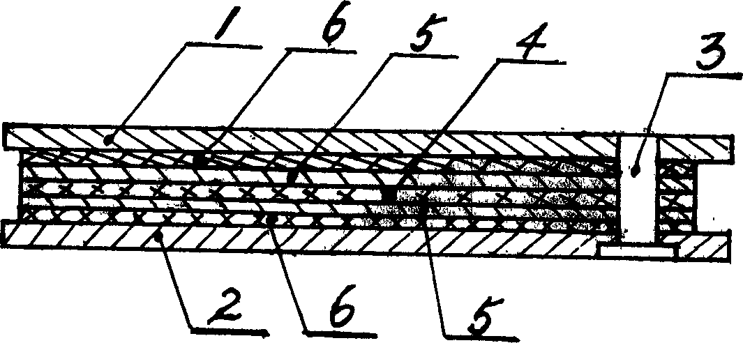
[0017] The specific implementation manner of the present invention will be described below by taking a four-layer circuit board as an example.

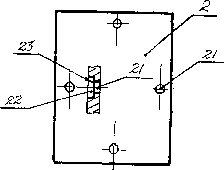
[0018] The lamination mold of multilayer circuit board of the present invention is made up of upper formwork 1, lower formwork 2, positioning pin 3, the thickness of upper formwork 1 and lower formwork 2 are 2 millimeters, and its material is high-quality pressure-resistant mirror stainless steel plate, four circular positioning holes 21 with countersunk holes 22 are arranged on the lower template 2, and the step surface 23 of the counterbore 22 is perpendicular to the axis of the positioning holes 21; four long waist holes are arranged on the upper template 1 11. The centers of the four long waist holes 11 correspond to the centers of the positioning holes 21 on the lower template 2, and the center line of the two long waist holes 11 is perpendicular to the center line of the other two long waist holes 11; The positioning pin 3 is a ...


PUM

PropertyMeasurementUnit
Thicknessaaaaaaaaaa

Abstract

The invention is made by means of following steps: takes high grade mirror surface stainless steel as material of lower mold plate and upper mold plate; the counter bore perpendicular to axial line of location hole is located at the bottom surface of location hole in the lower mold plate; the step locating pin is composed of the locating column and the foundation; the locating column is perpendicular to the foundation, and the upper mold plate and the lower mold plate are jointed through the step locating pin. Because the location holes in the lower mold plate and the up mold plate coincides with designing basis for each layer of circuit in multi layer circuit board, and is processed by using digital control equipment, the laminating mold has not only precise location, but also low weight, and can process 8 piece multi layer circuit board at on time by hot-pressed.

Description

Technical field: [0001] The invention relates to a lamination mold of a multilayer circuit board. Background technique: [0002] Multi-layer circuit boards are different from double-sided circuit boards. In multi-layer circuit boards, multi-layer circuit patterns are set, and the circuit patterns of each layer must be connected through predetermined connection holes. The manufacturing process is as follows: [0003] CAD and light painting→inner layer cutting→drilling positioning holes→scrubbing→coating photoresist→exposure→developing→etching→removing film→inner layer inspection→cleaning→inner layer blackening→lamination→NC drilling→ Hole inspection→hole pretreatment→copper sinking→copper layer inspection→graphic making→graphic plating→film removal→etching→lead and tin stripping→making solder mask graphics→curing→hot air leveling→printing character graphics→milling shape→cleaning and drying →Electrical testing→Baking plate→Finished product inspection→Packing and leaving the ...

Claims


Application Information

Patent Timeline
IPC IPC(8): H05K3/46H05K3/00H05K3/36
Inventor 李小元李进
Owner 李小元
Why Eureka
Try Eureka