Electromagnetic forbidden band structure material

A technology of electromagnetic band gap and microwave dielectric materials, which is applied in the structural form of radiation elements, circuits, electrical components, etc., can solve the problems of excessive size of planar unit cells, reduction of unit cell cycle number, discount, etc.

Inactive Publication Date: 2006-06-14
SHANGHAI FANGSHENG INFORMATION TECH +1
View PDF0 Cites 38 Cited by
  • Summary
  • Abstract
  • Description
  • Claims
  • Application Information

AI Technical Summary

Problems solved by technology

Although the above-mentioned two types of planar electromagnetic bandgap structure materials can provide sufficient bandgap frequency width to meet the application needs of most microwave components, the size of the planar unit cell is still too large when the substrate adopts a dielectric carrier with a low dielectric constant. Due to the limited geometric size requirements of components, the nu

Method used


Image

  • Electromagnetic forbidden band structure material
  • Electromagnetic forbidden band structure material
  • Electromagnetic forbidden band structure material

Examples


Embodiment Construction

[0013] For better understanding of the present invention, the present invention will now be further described with reference to the accompanying drawings.

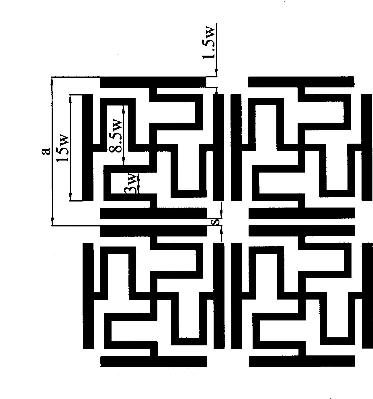
[0014] Electromagnetic band gap structure material pattern image 3 , the picture is a 2×2 arrangement of 4 unit cells. The printed circuit board process prints the metal pattern on the microwave dielectric material board. The metal can be copper, silver, aluminum, gold, etc., and the microwave dielectric material can be selected from PTFE. Vinyl and other materials, the black part in the figure represents metal, the specific size scale has been in image 3 It is marked in that the unit length w is determined by the applied frequency range, and different w values ​​correspond to different antenna operating frequency bands. According to different matching modes, the s value can be fine-tuned around the w value. In this embodiment, w=0.43 mm, s=w.

[0015] The volume of this material can be reduced by more than 50% compare...


PUM


Abstract

The invention provides a new, small-size, wide-band gap electromagnetic band gap structural material, and the manufacturing method prints special metal pattern on microwave medium material plate by PCB process, where the size of the pattern is determined according to the applied frequency range. The electromagnetic band gap structural material can be used in antennas, filters, resonators, and other microwave devices, to improve their performance.

Description

technical field [0001] The invention relates to an electromagnetic forbidden band structure, in particular to a novel electromagnetic forbidden band structure material with small size and wide forbidden band applied to radio frequency components. Background technique [0002] Electromagnetic Bandgap (EBG) or Photonic Bandgap (PBG) materials have broad application prospects in microwave and optical communications because of their unique properties of suppressing the propagation of electromagnetic waves at a certain frequency (segment). , has aroused widespread interest in recent years. According to the different arrangements of periodic structures, it can be divided into three categories: three-dimensional, two-dimensional (also called plane) and one-dimensional. Among them, the two-dimensional plane or quasi-planar structure is the most studied and reported in the existing literature due to its low profile and simple preparation process, and the typical representative is th...

Claims


Application Information

Patent Timeline
IPC IPC(8): H01Q1/38H01P1/20H01P1/23H01Q21/00
CPCH01P1/2005
Inventor 刘晓晗贺连星殷杰羿资剑李毅丁振宇
Owner SHANGHAI FANGSHENG INFORMATION TECH
Why Eureka
Try Eureka