Colour optical filter and its manufacturing method

A color filter and color filter technology, applied in the field of color filters, can solve the problems of voltage level attenuation, increase of production cost, lengthening of process time, etc., and achieve the effect of reducing conduction impedance

Inactive Publication Date: 2006-06-28
AU OPTRONICS CORP
View PDF0 Cites 2 Cited by
  • Summary
  • Abstract
  • Description
  • Claims
  • Application Information

AI Technical Summary

Problems solved by technology

The signal between the traditional silver glue points 15 is only transmitted by the electrode layer 13, but as the size of the panel increases, the voltage level between the silver glue points 15 will also attenuate with the increase of the conduction distance.
In the past, the solution to this phenomenon was to increase the coating thickness of the electrode layer to reduce the impedance or to increase the number of silver paste points to increase the conductivity, but these previous technologies often lead to longer process time and production costs. increase, this situation will have a greater impact if the panel size is designed and manufactured in the future

Method used


Image

  • Colour optical filter and its manufacturing method
  • Colour optical filter and its manufacturing method
  • Colour optical filter and its manufacturing method

Examples


no. 1 example

[0045] Please refer to the following Figure 3a to Figure 3d The process sectional view of the present invention is used to illustrate a preferred embodiment of the color filter and its manufacturing method.

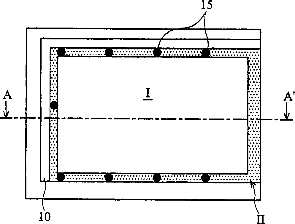
[0046] First, refer to Figure 3a , the present invention first provides a substrate 20, such as a plastic or glass substrate, and then forms a cover layer 21 to surround the sub-pixel unit 24. The material of the cover layer 21 includes black resin or black acrylic, and the cover layer 21 It can be produced by photolithography process (photo process), transfer process (transfer process), reverse printing process (Reverse printing), inkjet printing process (Inkjet printing) or DuPont laser printing method.

[0047] Then refer to Figure 3b , plate one or more layers of conductive layer 23 with sputtering method, electroless plating method, vapor deposition method or inkjet printing process (Inkjetprinting), and then utilize photomask to process photoetching etch, and t...

no. 2 example

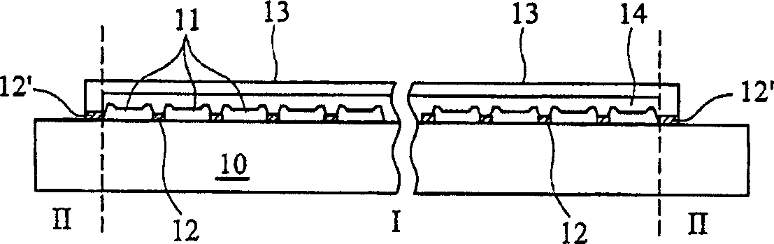
[0054] According to the color filter of the second preferred embodiment of the present invention and its manufacturing method, the difference from the first embodiment is that a flat layer 25 is formed before the electrode layer 26 is formed, such as Figure 4a As shown, the covering layer 21 and the color filter unit 22 are firstly formed according to the method of the first embodiment.

[0055] Then refer to Figure 4b , form a flat layer 25 on the color filter unit, the flat layer 25 can fully cover the cover layer 21 and the color filter unit 22, and this flat layer 25 can be a thermosetting photoresist or a UV photohardening photoresist composed of resist, then refer to Figure 4c , form a plurality of strips or matrix conductive layers 23 above the cover layer 21 by sputtering, evaporation, inkjet printing or electroless plating, and correspond to the cover layer 21, finally refer to Figure 4d Form a layer of electrode layer 26 on the substrate 20 by sputtering or non...

no. 3 example

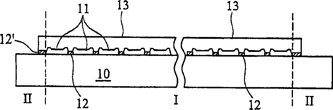
[0057] According to the color filter of the third preferred embodiment of the present invention and its manufacturing method, the difference from the second embodiment is that the conductive layer 23 is formed first, and then the flat layer 25 is formed. Therefore, the flat layer 25 must have The contact hole (via hole) 27 is used to conduct the electricity between the conductive layer 23 and the electrode layer 26 .

[0058] First, after completing the cover layer 21, the color filter unit 22 and the conductive layer 23 according to the second embodiment, as Figure 3c shown, then refer to Figure 5a , after forming a flat layer 25 on the color filter unit 22 and the conductive layer 23 in an all-round way, on the flat layer 25, use a photolithographic etching process or a non-photomask technology (Laser Writing, EUV Writing, Electron-Beam or Ion-Beam ) define more than one contact hole (via hole) 27 so that the conductive layer 23 is exposed, and finally refer to Figure 5...


PUM


Abstract

A color filter is featured as adding one or multiple conductive layer above covering layer between R / G / B color filtering units on color filter to form parallel structure being connected through to each other and being set between conductive layer and electrode layer, utilizing said parallel structure to decrease transmission impedance.

Description

technical field [0001] The invention relates to a color filter, in particular to a structure and a manufacturing method of the color filter. Background technique [0002] Figure 1a It is a schematic diagram of the plane structure of a general traditional color filter. Among them, cut a section along A-A', such as Figure 1b As shown, it includes display area I and non-display area II, wherein display area I includes substrate 10, R / G / B color resistance 11, cover layer (display area I) 12, flat layer (Overcoat Layer) 14 and electrode layer 13. The electrode layer 13 can be ITO or other transparent conductive oxides (TCO) under development, such as AZO, etc., wherein the non-display area II also includes a cover layer (non-display area II) 12'. As the size of the panel increases, the voltage level will attenuate with the conduction distance, resulting in insufficient regional voltage level. At present, the general solution to this phenomenon can be achieved by increasing t...

Claims


Application Information

Patent Timeline
Patent Type & Authority Applications(China)
IPC IPC(8): G02B5/23
Inventor 黄彦衡刘佑玮丁友信黄国有
Owner AU OPTRONICS CORP
Why Eureka
Try Eureka