

Collet, chip bonder and chip pick-up method
A collet and chip technology, applied in chucks, electrical components, manipulators, etc., can solve the problems of cracking and easy occurrence of chip chips, and achieve the effect of preventing splitting
- Summary
- Abstract
- Description
- Claims
- Application Information
AI Technical Summary
Problems solved by technology
Method used
Image

Examples
Embodiment 1
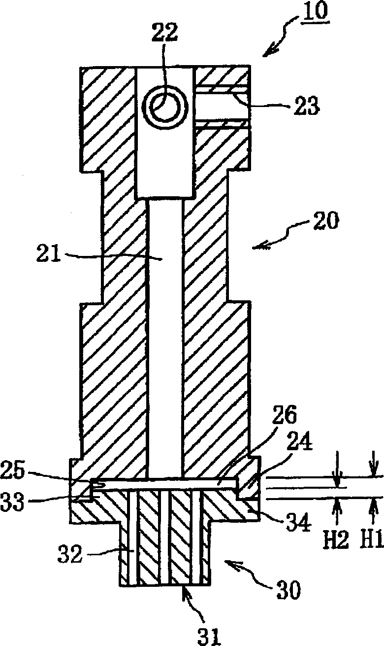
[0094] About the tool 10 of the first embodiment of the present invention such as Figure 1A~Figure 1C As shown, there is a collet holder 20 and a collet 30 mounted on the collet holder 20. The collet holder 20 is made of, for example, stainless steel, and has a vacuum suction hole 21 connected to a vacuum system at its center, and has two mounting screw holes 22 for mounting the collet holder 20 on a supporting member, 23. A descending portion 24 in the peripheral portion of the lower peripheral portion, and a recess 25 surrounded by the descending portion 24.
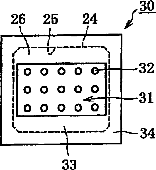
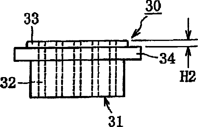
[0095] The collet 30 is made of stainless steel, nitrile rubber, fluorine rubber, heat-resistant resin, etc. depending on the application. It has a flat surface 31 on the bottom and a large number of penetrating through (Figure Examples are rectangular sheet chips, 3 vertical x 5 horizontal 15) small diameter vacuum suction holes 32, convex portions 33 embedded in the recesses 25 of the collet holder 20, and the collet ho...
Embodiment 2
[0104] Hereinafter, referring to the collet 10A of the second embodiment of the present invention, refer to Figure 3A , Figure 3B , Figure 3C Be explained. The collet 10A includes a collet holder 20 and a collet 30A. Collet holder 20 with Figure 1A The collet holders 20 shown are the same, so the same reference numerals are given to the same parts, and the description thereof is omitted.
[0105] The collet 30A has a flat surface 31 below, a plurality of small diameter vacuum suction holes 32, a convex portion 33 embedded in the recess 25 of the collet holder 20, and abuts against the lower surface of the descending portion 24 of the collet holder 20 Of the flange portion 34, and Figure 1A The collet 30 is the same, but the difference is that it also has a plurality of grooves 35 communicating with the lower end of the vacuum suction hole 32 in one direction, and a plurality of grooves communicating with the lower end of the vacuum suction hole 32 in the other direction.部36. ...
PUM
 Abstract
Description
Claims
Application Information