Display panel with repairing line and signal line set on differential substrates

A technology for display panels and repair wires, applied in nonlinear optics, identification devices, instruments, etc., can solve problems such as limited space for repair wires, high resistance, and reduced success rate of wires, and achieve strong repair capabilities and low resistance- Capacitive delay effect, effect of reducing power loss

Active Publication Date: 2006-08-30
AU OPTRONICS CORP
View PDF0 Cites 9 Cited by
  • Summary
  • Abstract
  • Description
  • Claims
  • Application Information

AI Technical Summary

Problems solved by technology

Because the path of signal transmission is too long and the resistance value is too high, it is easy to generate resistance-capacitance delay effect (RC delay effect) between the liquid crystal layer, which reduces the success rate of repairing the wires with open circuit phenomenon, and increases the power of the liquid crystal display panel 10. loss
[0006] In the structure of the liquid crystal display panel 10 in the known technology, the data lines D1-Dm, the scan lines S1-Sn and the repair lines T1-Ts are all arranged on the thin film transistor substrate. In order not to affect the operation of the pixels, the repair lines T1-Ts It needs to be arranged outside the display area 20 so that the length of the repair line T1-Ts is much longer than the length of the data line D1-Dm. Therefore, the resistance of the signal transmission path provided by the repair line T1-Ts in the known technology is too high, and it is easy to contact with the liquid crystal layer. The resistance-capacitance delay effect will be generated between them, the success rate of repairing the open circuit phenomenon will be reduced, and the power loss of the liquid crystal display panel 10 will be increased.
In addition, components such as data lines, scanning lines, and driving circuits have been placed on the thin film transistor substrate, leaving limited space for repair lines
Therefore, the liquid crystal display panel 10 of the known technology can only provide a limited number of repair lines, and the repair capability is insufficient.

Method used


Image

  • Display panel with repairing line and signal line set on differential substrates
  • Display panel with repairing line and signal line set on differential substrates
  • Display panel with repairing line and signal line set on differential substrates

Examples


Embodiment Construction

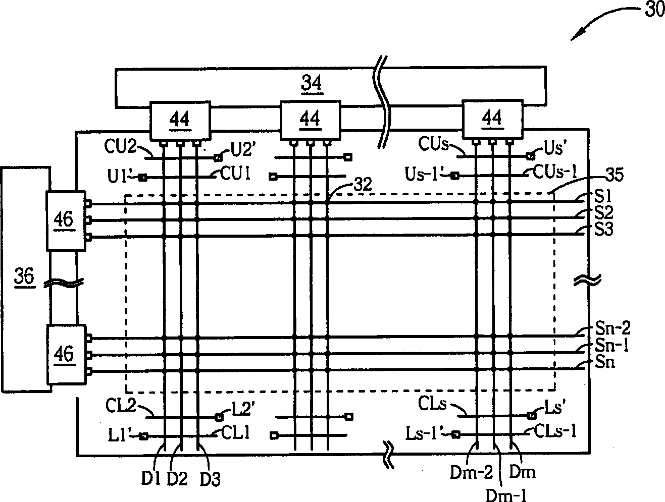
[0037] In the invention, the signal line of the liquid crystal display panel is arranged on the thin film transistor substrate, and the repair line of the liquid crystal display panel is arranged on the optical filter substrate. Please refer to image 3 and Figure 4 , image 3 It is a top view of a thin film transistor substrate 30 of a liquid crystal display panel 50 in the present invention, Figure 4 It is a plan view of the filter substrate 40 of the liquid crystal display panel 50 .

[0038] exist image 3 Among them, a plurality of data lines D1-Dm parallel to each other and a plurality of scan lines S1-Sn parallel to each other are arranged on the display area 35 of the thin film transistor substrate 30 . The data lines D1-Dm and the scan lines S1-Sn intersect with each other and form a pixel matrix 32 . Each pixel in the pixel matrix 32 and its corresponding pixel drive circuit composed of electronic components such as thin film transistors and capacitors are com...


PUM


Abstract

The invention relates to a display panel that the mending line and signal line set on different base board. The display panel includes a mending line to take place of the broken signal line. Plural signal lines are set on the first side of the first base board of display panel. And plural mending lines are set on the first side of second base board of display panel. The first side of the second base board is faced to the first side of the first base board. A liquid crystal layer is set between the first base board and the second base board. The invention could effectively decrease resistance-capacitance delay effect and power consumption of liquid display panel.

Description

technical field [0001] The present invention relates to a display panel, in particular to a liquid crystal display panel in which repair lines and signal lines are arranged on different substrates. Background technique [0002] Liquid crystal displays are widely used in portable information products such as notebook computers, personal digital assistants (PDAs), digital cameras, and video cameras due to their thin and light appearance, low power consumption, and no radiation pollution. , the liquid crystal display has gradually replaced the traditional cathode ray tube (cathode ray tube, CRT) display. [0003] A general liquid crystal display panel structure includes a thin-film transistor substrate (thin-film transistor substrate, TFT substrate), a color filter substrate (color filter substrate, CF substrate) and a liquid crystal layer disposed between the two substrates. The thin film transistor substrate includes a pixel matrix (pixel matrix) composed of multiple rows of...

Claims


Application Information

Patent Timeline
Patent Type & Authority Applications(China)
IPC IPC(8): G02F1/13G09F9/00G02F1/1335
Inventor 廖启南
Owner AU OPTRONICS CORP
Why Eureka
Try Eureka