Apparatus including 4-way valve for fabricating semiconductor device, method of controlling valve, and method of fabricating semiconductor device using the apparatus

A technology for semiconductors and devices, applied in the field of devices for manufacturing semiconductor devices, can solve the problems of slow diffusion and release of source gas materials, difficulty in ALD, and inability to completely remove them, and achieve the effect of improving purging efficiency

Active Publication Date: 2006-08-30
SAMSUNG ELECTRONICS CO LTD +1
View PDF2 Cites 10 Cited by
  • Summary
  • Abstract
  • Description
  • Claims
  • Application Information

AI Technical Summary

Problems solved by technology

[0026] Source gas material remaining in the DV section may diffuse and release slowly, but is not completely removed, even after a few minutes
Considering the ALD cycle which lasts several seconds, it is difficult to perform ALD without purging and removing various source gases remaining in the DV section

Method used


Image

  • Apparatus including 4-way valve for fabricating semiconductor device, method of controlling valve, and method of fabricating semiconductor device using the apparatus
  • Apparatus including 4-way valve for fabricating semiconductor device, method of controlling valve, and method of fabricating semiconductor device using the apparatus
  • Apparatus including 4-way valve for fabricating semiconductor device, method of controlling valve, and method of fabricating semiconductor device using the apparatus

Examples


Embodiment Construction

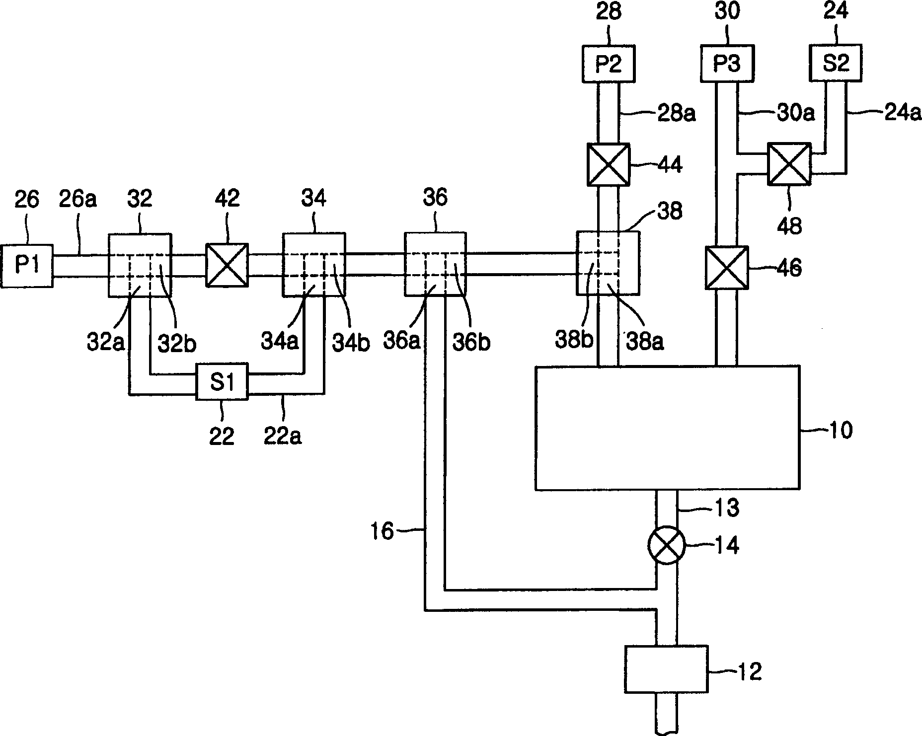
[0054] The present invention can be applied to basically any apparatus that supplies a gaseous material to a reaction chamber and performs a semiconductor manufacturing process in the reaction chamber using the gaseous material. Therefore, the present invention can be widely applied to deposition equipment, such as chemical vapor deposition (CVD) or atomic layer deposition (ALD) equipment, and etching equipment. The following exemplary embodiments of the invention will be described below in connection with ALD, but the invention is also applicable to other processes.

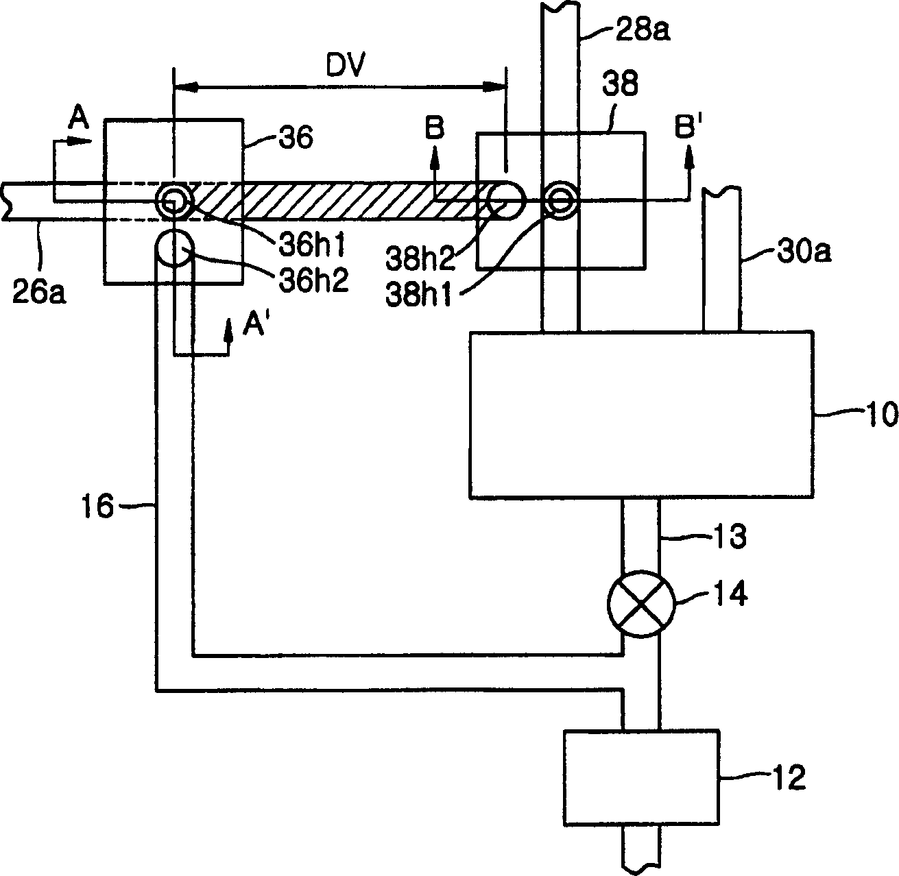
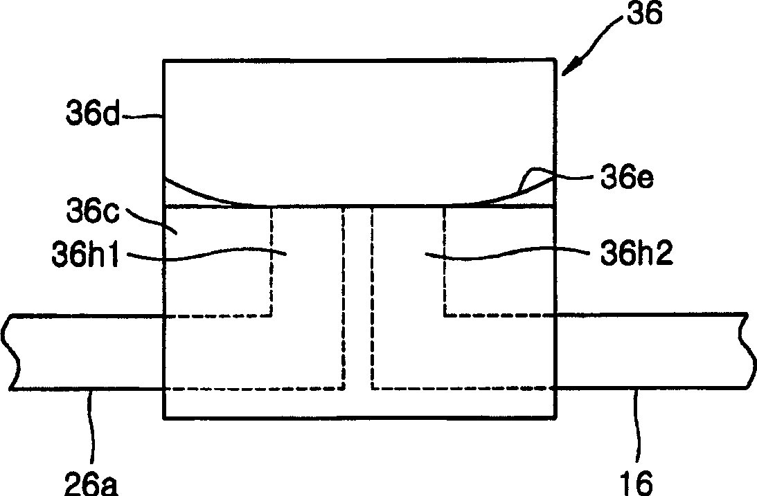
[0055] Figure 5 is a schematic diagram illustrating an apparatus for manufacturing a semiconductor device according to a first embodiment of the present invention. Image 6 yes Figure 5 Enlarged view of part of the device shown. Figure 7is along Image 6 The section shown is a cross-sectional view taken along line CC' where the 2-way valve is closed. Figure 8 is along Image 6 A cross-sectional view ta...


PUM


Abstract

An apparatus and method for fabricating a semiconductor device using a 4-way valve with improved purge efficiency by improving a gas valve system by preventing dead volume from occurring are provided. The apparatus includes a reaction chamber in which a substrate is processed to fabricate a semiconductor device; a first processing gas supply pipe supplying a first processing gas into the reaction chamber; a 4-way valve having a first inlet, a second inlet, a first outlet, and a second outlet and installed at the first processing gas supply pipe such that the first inlet and the first outlet are connected to the first processing gas supply pipe; a second processing gas supply pipe connected to the second inlet of the 4-way valve to supply a second processing gas; a bypass connected to the second outlet of the 4-way valve; and a gate valve installed at the bypass.

Description

technical field [0001] The present invention relates to an apparatus for manufacturing semiconductor devices, and more particularly, to an apparatus for employing a 4-way valve by improving the valve system for supplying gas to a reaction chamber with improved purge (purge) An apparatus for efficiently manufacturing a semiconductor device, a method for controlling the 4-way valve, and a method for manufacturing a semiconductor device using the apparatus. Background technique [0002] Semiconductor devices are manufactured by repeatedly performing processes such as deposition and patterning of thin layers on the surface of a substrate, that is, a wafer. Deposition and patterning of the thin layers is typically done in a semiconductor processing module. The configuration of a semiconductor processing module varies depending on the process used in the process of manufacturing semiconductor devices, but it basically includes a reaction chamber defining a reaction area in which ...

Claims


Application Information

Patent Timeline
Patent Type & Authority Applications(China)
IPC IPC(8): H01L21/00H01L21/67H01L21/3065H01L21/205C23C16/44C23F4/00
CPCF04C29/0092F16K7/00G05D7/00H01L21/0228H01L21/67034H01L21/67207
Inventor 元皙俊刘龙珉金大渊金永勋权大振金元洪
Owner SAMSUNG ELECTRONICS CO LTD
Why Eureka
Try Eureka