Step scan photo-etching machine double-platform exchanging and positioning system
A positioning system and step-scanning technology, which is applied in the direction of optomechanical equipment, microlithography exposure equipment, optics, etc., can solve the problems of increased cost, very high precision requirements, increased system manufacturing costs, etc., to reduce time-consuming, reduce Cost, the effect of effective cost control
- Summary
- Abstract
- Description
- Claims
- Application Information
AI Technical Summary
Problems solved by technology
Method used
Image

Examples
Embodiment Construction
[0038] The present invention will be described in detail below in conjunction with the accompanying drawings and specific embodiments.
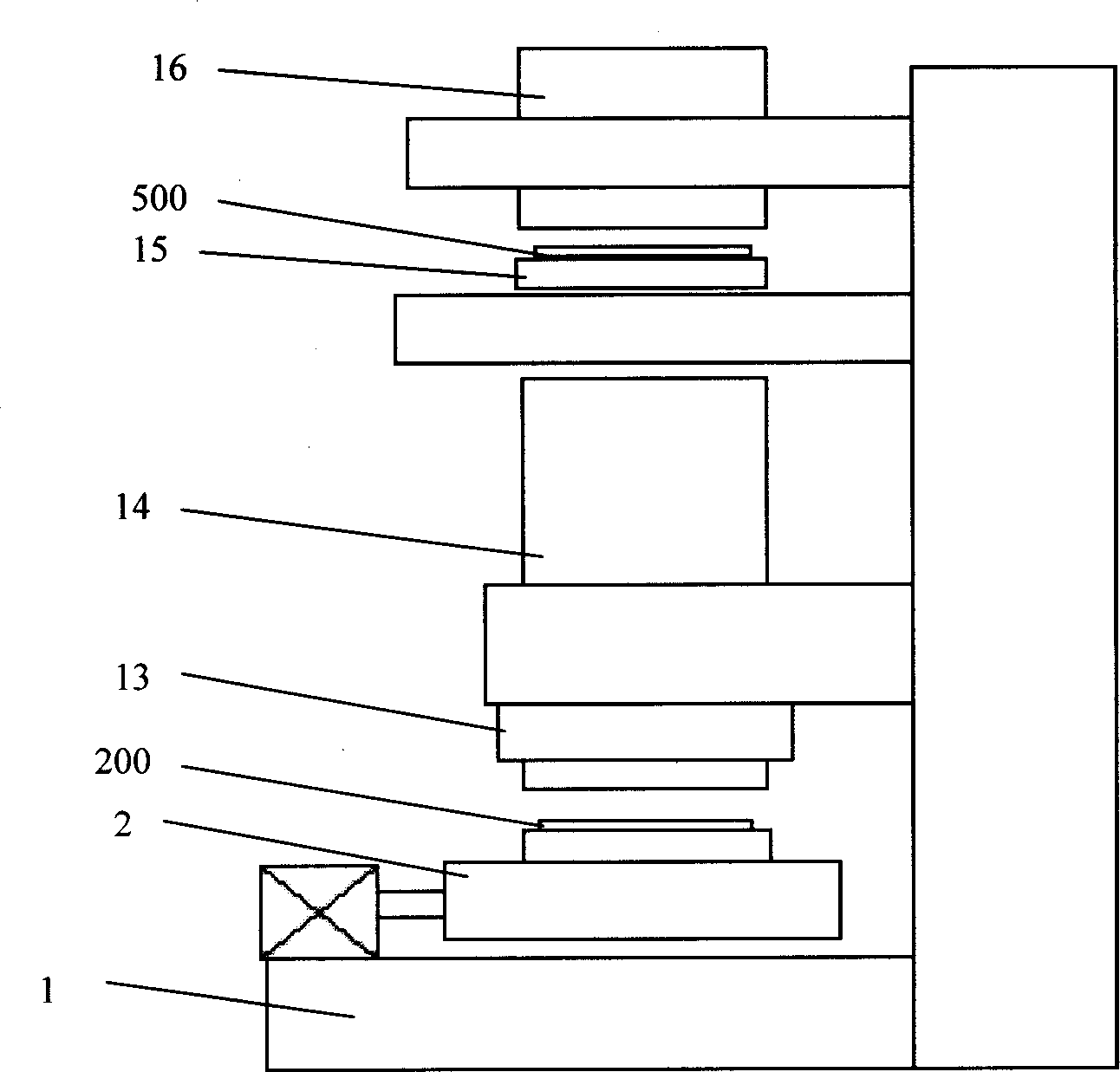
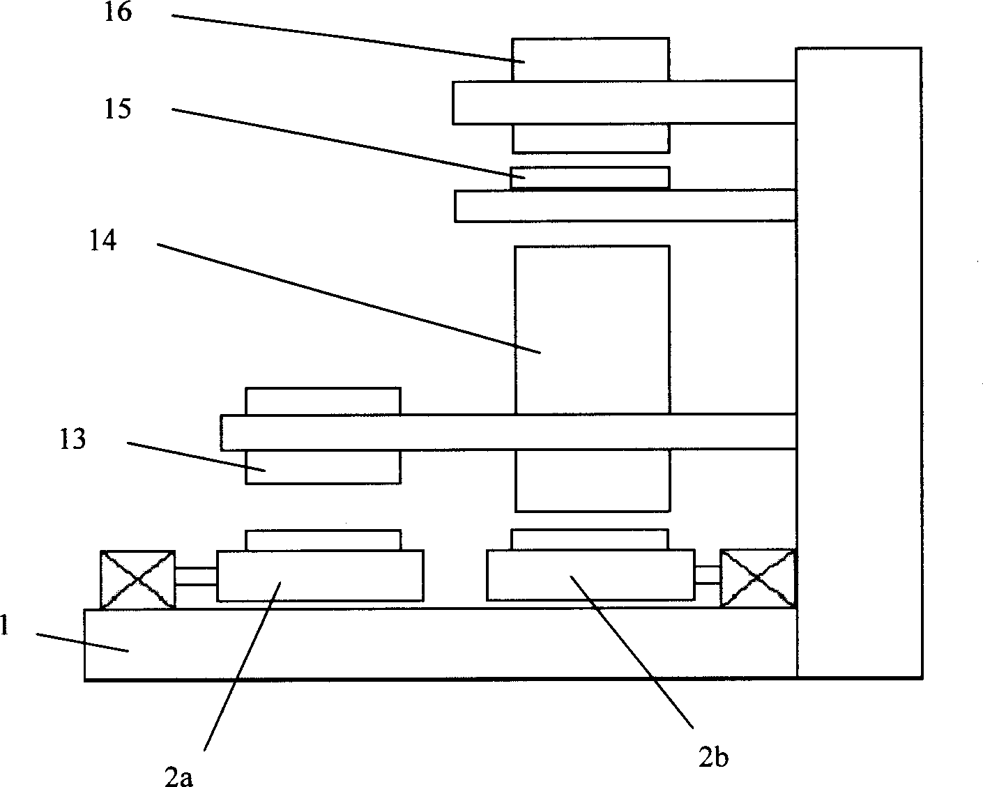
[0039] Figure 5It shows the working state of the dual wafer stage positioning system of the present invention, and its structure includes a total base 1, a wafer stage positioning unit arranged on the total base and operating at the exposure station, and a wafer stage positioning unit operating at the pretreatment station Wafer stage positioning unit, each wafer stage positioning unit includes silicon wafer carrier device 2a (silicon wafer carrier device for pretreatment station), 2b (silicon wafer carrier device for exposure station), motion positioning detection device 50a, 51a , 50b, 51b; x guide rail 10a, or 10b, 11b; y guide rail 20a, 21a or 20b, 21b, each silicon chip carrier is installed on the x guide rail, can move along the x guide rail, x guide rail installation On the y guide rail and can move along the y guide rail, the x guide...
PUM
 Abstract
Description
Claims
Application Information
 - Generate Ideas
- Intellectual Property
- Life Sciences
- Materials
- Tech Scout
- Unparalleled Data Quality
- Higher Quality Content
- 60% Fewer Hallucinations
Browse by: Latest US Patents, China's latest patents, Technical Efficacy Thesaurus, Application Domain, Technology Topic, Popular Technical Reports.
© 2025 PatSnap. All rights reserved.Legal|Privacy policy|Modern Slavery Act Transparency Statement|Sitemap|About US| Contact US: help@patsnap.com