Testing clamp and method of producing super-short optical palse based on cascade electrical sucking modulator

A technology of electro-absorption modulator and test fixture, which is applied in the direction of instruments, measuring electronics, measuring devices, etc., and can solve problems such as complicated operation, high-frequency probes are expensive, and easy to be damaged

Inactive Publication Date: 2006-09-20
INST OF SEMICONDUCTORS - CHINESE ACAD OF SCI
View PDF0 Cites 7 Cited by
  • Summary
  • Abstract
  • Description
  • Claims
  • Application Information

AI Technical Summary

Problems solved by technology

The disadvantage is that the operation is complicated, an

Method used


Image

  • Testing clamp and method of producing super-short optical palse based on cascade electrical sucking modulator
  • Testing clamp and method of producing super-short optical palse based on cascade electrical sucking modulator
  • Testing clamp and method of producing super-short optical palse based on cascade electrical sucking modulator

Examples


Embodiment

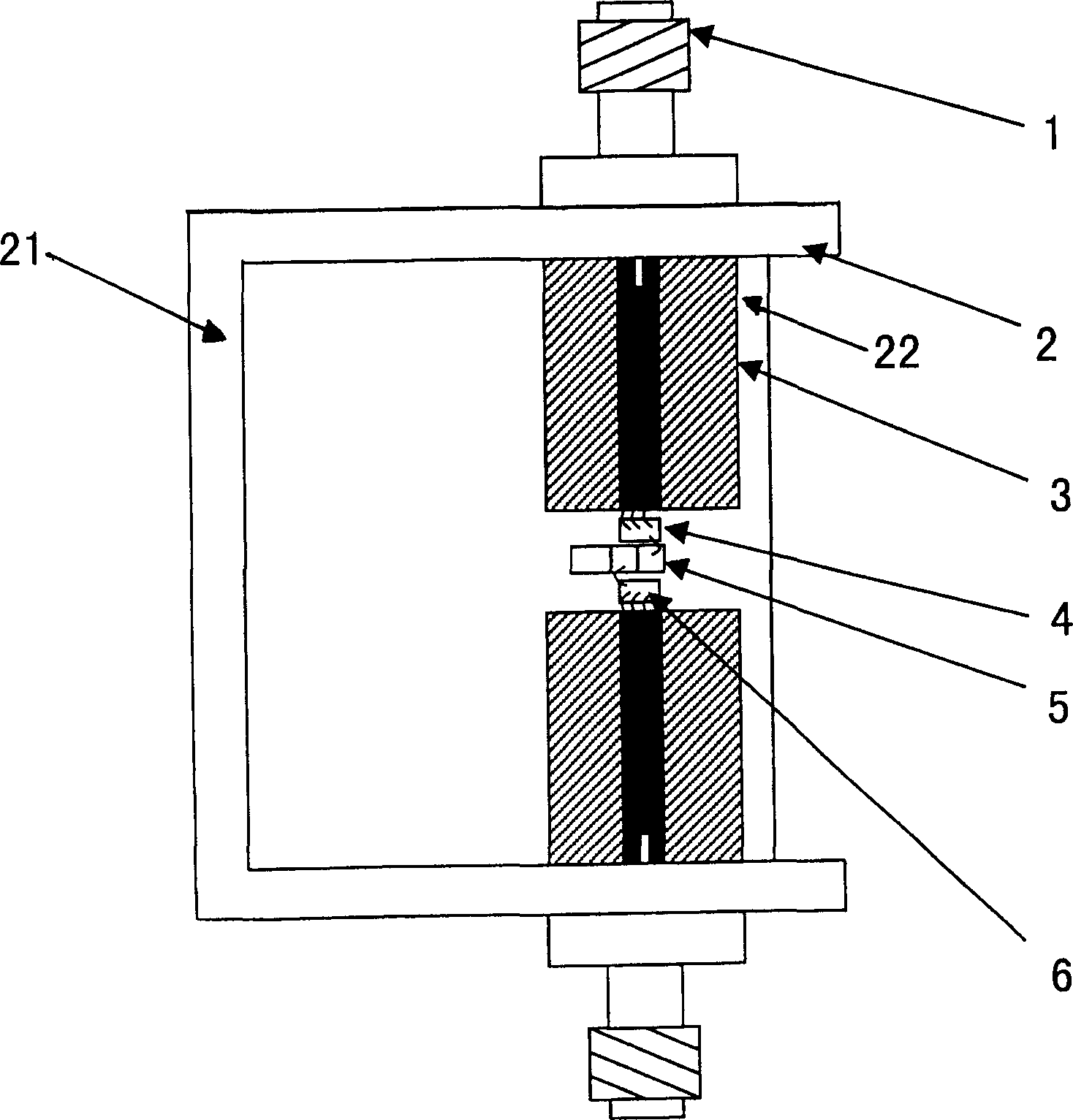
[0041] Such as figure 1 , figure 2 , image 3 , Figure 4 As shown, a test fixture and method for generating ultrashort optical pulses based on cascaded electroabsorption modulators of the present invention, including:

[0042] (1) Design and make test and calibration fixture 2; test and calibration fixture 2 can be made of aluminum or copper, but the surface must be plated with gold, because the excellent conductivity of gold can reduce microwave loss ( figure 1 );

[0043] (2) Design and manufacture the microstrip line 3 . The metal material of the microstrip line 3 can be copper, but the surface must be plated with gold. Due to the excellent conductivity of gold, microwave loss and reflection can be reduced, and the same material as the chip bonding wire (gold wire 6) is easy to solder. The dielectric substrate of the microstrip line 3 can be selected from materials such as ceramics, composite dielectric or polytetrafluoroethylene, and the thickness of the substrate i...


PUM

PropertyMeasurementUnit
Resistanceaaaaaaaaaa

Abstract

The invention relates to a testing clamping device based on cascade electric adsorbing modulator to generate super short light pulse. The feature is that it includes a frame, a base board, two radio frequency coaxial connectors, two sections of micro strips and two resistances that is fixed between two ends of the micro strips and has a preset distance.

Description

technical field [0001] The present invention relates to a test fixture and method for generating ultra-short optical pulses based on a cascaded electroabsorption modulator, in particular to a distributed feedback semiconductor laser (DFB-LD) and a cascaded electroabsorption modulator ( EAM) measurement of ultrashort light pulses generated by monolithically integrated chips. Background technique [0002] Ultra-high-speed and large-capacity optical fiber communication is the main direction of optical communication research in recent years. Optical Time Division Multiplexing (OTDM) is one of the effective ways to overcome the bottleneck of optical and electrical devices and realize ultra-high-speed optical fiber communication. High repetition rate frequency conversion limit ultrashort optical pulse source is the core device to realize optical soliton communication and OTDM optical communication, and it is also an indispensable basis for other key technology research. The dist...

Claims


Application Information

Patent Timeline
IPC IPC(8): G01J11/00G01R31/00
Inventor 赵谦潘教青王圩
Owner INST OF SEMICONDUCTORS - CHINESE ACAD OF SCI
Why Eureka
Try Eureka