Image recovery and pupil filtering type transverse super-resolution confocal microscopic imaging method and apparatus

A confocal microscopy imaging, pupil filtering technology, applied in microscopes, optics, optical components, etc., can solve problems such as high cost, technology and system complexity

Inactive Publication Date: 2006-09-27
HARBIN INST OF TECH
View PDF2 Cites 12 Cited by
  • Summary
  • Abstract
  • Description
  • Claims
  • Application Information

AI Technical Summary

Problems solved by technology

[0005] Generally speaking, the above-mentioned first and second types of methods and technologies belong to the category of optical super-resolution, which are mainly realized by changing the optical path layout of the confocal microscope, adding super-resolution pupil filte

Method used


Image

  • Image recovery and pupil filtering type transverse super-resolution confocal microscopic imaging method and apparatus
  • Image recovery and pupil filtering type transverse super-resolution confocal microscopic imaging method and apparatus
  • Image recovery and pupil filtering type transverse super-resolution confocal microscopic imaging method and apparatus

Examples


Embodiment Construction

[0047] The image restoration and pupil filter type lateral super-resolution confocal microscopic imaging method and device of the present invention are described in detail in combination with embodiments and accompanying drawings as follows:

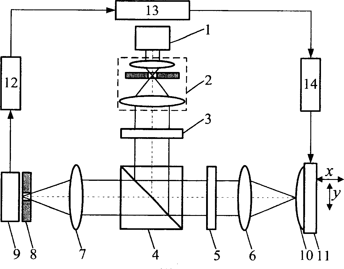
[0048] The system device of Embodiment 1 of the present invention is as figure 2 As shown, it includes a light source 1, a collimating beam expander 2, a pupil filter 3, a polarization beam splitter 4 placed on the light source emitting end in turn, a 1 / 4 wave plate 5 placed on the reflection light path of the polarization beam splitter 4, and a display Micro-objective lens 6, and the condenser lens 7 that is placed on the polarizing beam splitter 4 transmitted light paths and the pinhole 8 that is positioned at the focal point of condenser lens 7, and the CCD detector 9 that is close to the pinhole 8 back, also includes follow CCD detector 9 connected image acquisition card 12, a computer measurement control and image processing system...


PUM


Abstract

This invention relates to an image recovery and pupil filtering type transverse super-resolution confocal microscopic imaging method and apparatus, which comprises a light source (1) with a collimated beam expander (2) and a pupil filter (3), a split-beam polarizer (4) with a 1/4 plate (5) and a microscopic objective lens (6) both on reflection path and a collecting lens (7) on transmitted path that comprises a pinhole (8) on focus of (7) and a CCD probe (9) behind (8). This invention improves system lateral resolution and has wide application.

Description

technical field [0001] The invention belongs to the technical field of microscopic imaging and microscopic precision measurement, in particular to a method and device for realizing super-resolution imaging detection. Background technique [0002] With the rapid development of the world's information industry, breakthroughs have been made in microelectronics manufacturing technology, and processing precision, integration and reliability of VLSI chips have been continuously improved. After experiencing the mark sizes of 0.25μm, 0.18μm, and 0.13μm, the line width of integrated circuits has reached 90nm, and has begun to move towards the processing technology of 45nm and 22nm line width. Various geometric parameters such as line width, line spacing, step height, and film thickness in integrated circuits have become important parameters that affect device quality and yield. When the integrated circuit line width reaches below 0.1 μm, it marks that semiconductor manufacturing tec...

Claims


Application Information

Patent Timeline
IPC IPC(8): G02B21/00
Inventor 赵维谦邱丽荣冯政德陈珊珊
Owner HARBIN INST OF TECH
Why Eureka
Try Eureka