Integrated optical metrology and lithographic process system for dynamic critical dimension control

A lithography process and process technology, which is applied in the direction of optics, photolithography process exposure devices, semiconductor/solid-state device manufacturing, etc., can solve the problems of general products without structure and inconvenience, increase process capacity and yield, and reduce process stoppage The number of times, the effect of improving production capacity and yield rate

Active Publication Date: 2006-10-04
TAIWAN SEMICON MFG CO LTD
View PDF0 Cites 4 Cited by
  • Summary
  • Abstract
  • Description
  • Claims
  • Application Information

AI Technical Summary

Problems solved by technology

[0007] It can be seen that the lithography process of the above-mentioned existing semiconductor elements obviously still has inconvenience and defects in the manufacturing method and use, and needs to be further improved urgently.
In order to solve the problems existing in the lithography process of the existing semiconductor components, the relevant manufacturers have tried their best to find a solution, but no suitable design has been developed for a long time, and there is no suitable structure for general products. To solve the above problems, this is obviously a problem that the relevant industry is eager to solve

Method used


Image

  • Integrated optical metrology and lithographic process system for dynamic critical dimension control
  • Integrated optical metrology and lithographic process system for dynamic critical dimension control
  • Integrated optical metrology and lithographic process system for dynamic critical dimension control

Examples


Embodiment Construction

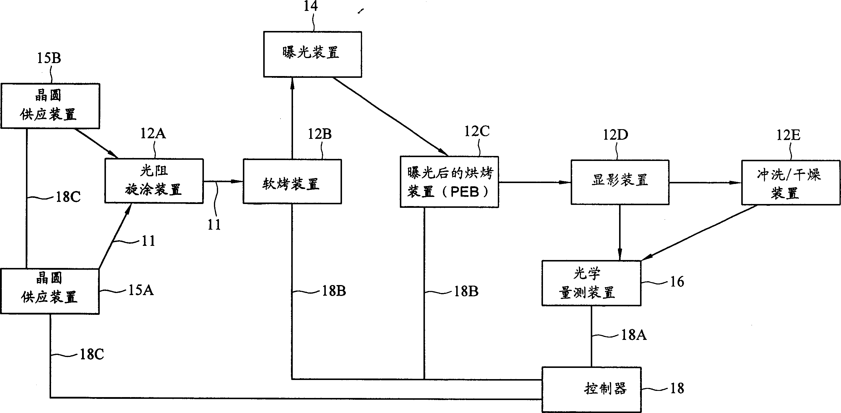
[0045] In order to further illustrate the technical means and effects of the present invention to achieve the intended purpose of the invention, the integrated optical measurement and lithography proposed according to the present invention for dynamically controlling the feature size will be described below in conjunction with the accompanying drawings and preferred embodiments. The specific implementation, structure, steps, features and functions of the manufacturing process system are described in detail below.

[0046] Although the implementation of the present invention is illustrated by improving the accuracy and uniformity of the feature size of the patterned photoresist layer in an integrated circuit as an example, the present invention is also applicable to the application field of Micro-engineered Machine, and is also applicable to A photoresist pattern whose feature dimension line width is less than 0.25 microns is used to perform subsequent dry etching process using ...


PUM

PropertyMeasurementUnit
diameteraaaaaaaaaa

Abstract

A method and apparatus for improving a yield and throughput of a lithographic process track, the method including providing a first resist layer on a first process wafer; forming a first resist pattern in the first resist layer including a heating process according to a first temperature profile wherein the heating process comprises a plurality of temperature controllable heating zones; producing and collecting scattered light spectra from the first resist pattern processing the scattered light spectrum to obtain 3-dimensional information including first resist pattern critical dimensions; determining a second temperature profile for performing the heating process to achieve targeted resist pattern critical dimensions including a second resist pattern on a second process wafer; and, forming the second resist pattern dimensions including the heating process according to the second temperature profile.

Description

technical field [0001] The present invention relates to a lithography process, in particular to a treatment method for photoresist baking and development in the integrated circuit production process. The treatment method includes integrating a temperature control device and an optical measurement system. A method is used to adjust the photoresist baking process to improve the critical-dimension (CD) in the lithography process and control the uniformity of the feature size to increase the throughput of the wafer. Background technique [0002] Due to the rapid development of semiconductor elements, the size of semiconductor elements continues to shrink, making the size of semiconductor wafers smaller and smaller, and effectively increasing the density of semiconductor elements. As the size of semiconductors continues to shrink and develop towards high density, the limiting factor gradually changes to the need to improve the accuracy of the lithographic patterning process and t...

Claims


Application Information

Patent Timeline
Patent Type & Authority Applications(China)
IPC IPC(8): G03F7/20G03F7/00H01L21/027
CPCG03F7/70625A47J27/0802A47J27/09A47J36/06
Inventor 柯志明游信胜王育溪高蔡胜黄得智
Owner TAIWAN SEMICON MFG CO LTD
Why Eureka
Try Eureka