Semiconductor device manufacturing method

A manufacturing method and semiconductor technology, applied in semiconductor/solid-state device manufacturing, semiconductor devices, semiconductor/solid-state device components, etc., can solve problems such as difficulty in obtaining strength, difficulty in forming slit hole alignment, etc., and achieve reduction in the number of processes Effect

Inactive Publication Date: 2006-10-04
SANYO ELECTRIC CO LTD
View PDF1 Cites 44 Cited by
  • Summary
  • Abstract
  • Description
  • Claims
  • Application Information

AI Technical Summary

Problems solved by technology

[0011] However, in the semiconductor device of the above-mentioned chip size package, since the semiconductor substrate 60 is separated by the slit hole 80, it is necessary to support and fix it on the same plane by the resin layer 78, but since it is bonded to the insulating film 74, and It has a uniform thickness, so there is a big practical problem that it is difficult to obtain sufficient strength
[0012] In addition, since the slit hole 80 is formed from the back surface of the semiconductor substrate 80, there is also a problem that there is no mark as a reference, and it is difficult to perform alignment when forming the slit hole.

Method used


Image

  • Semiconductor device manufacturing method
  • Semiconductor device manufacturing method
  • Semiconductor device manufacturing method

Examples


Embodiment Construction

[0050] Hereinafter, the best mode for carrying out the present invention will be described in detail with reference to the drawings.

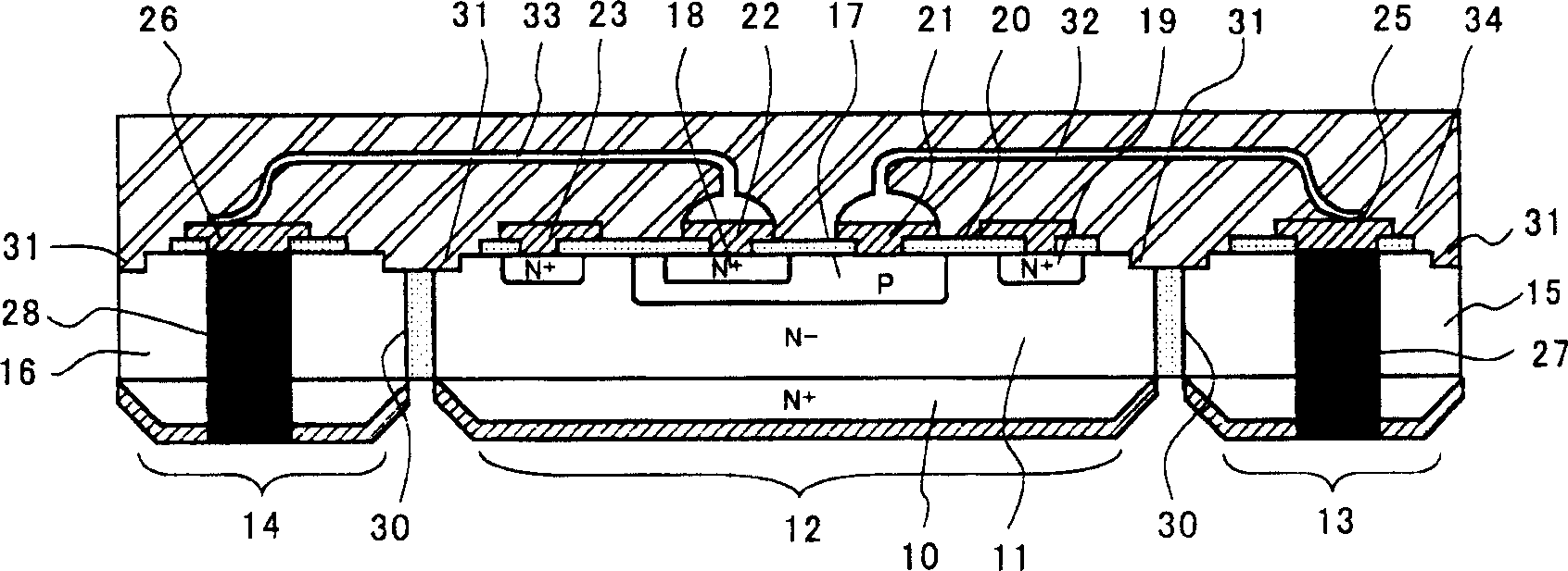
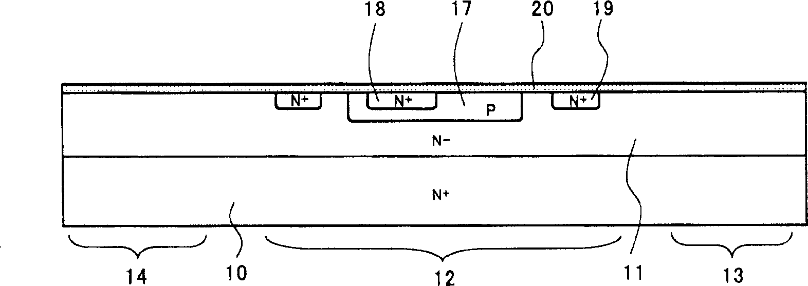
[0051] figure 1 It is a cross-sectional view illustrating a semiconductor device completed by the manufacturing method of the present invention. Figure 2 to Figure 9It is a cross-sectional view illustrating a method of manufacturing a semiconductor device of the best mode for carrying out the present invention, Figure 10 It is a plan view illustrating an arrangement relationship of electrodes of a semiconductor device of the best form for carrying out the present invention.

[0052] Such as figure 1 As shown, the semiconductor device completed by the manufacturing method of the present invention has: a semiconductor substrate, which has a first region and a second region; a plurality of electrodes, which are connected to the circuit element provided in the first region and the circuit element ; an electrode for external connection, which...


PUM


Abstract

By simultaneously forming via holes 35 for forming through electrodes 27 and 28 to be provided in second regions 13 and 14 and isolation trenches 30 for separating a first region 12 from the second regions 13 and 14 , positioning of the via holes 35 and the isolation trenches 30 is omitted.

Description

technical field [0001] The present invention relates to a method for manufacturing a semiconductor device, in particular to a method for manufacturing a semiconductor device packaged with wafer-level chips. Background technique [0002] Generally, a semiconductor device having transistor elements formed on a silicon substrate uses Figure 11 structure shown. 1 is a silicon substrate, 2 is an island-shaped portion such as a heat sink on which the silicon substrate 1 is mounted, 3 is a lead terminal, and 4 is a sealing resin. [0003] Such as Figure 11 As shown, the silicon substrate 1 formed with the transistor element is fixedly installed on the island-shaped part 2 such as the heat dissipation plate of the copper base material through the solder 5 such as solder, and the base electrode and the emitter electrode of the transistor element are arranged on the silicon substrate by bonding wires. Lead terminals 3 around the substrate 1 are electrically connected. Lead termina...

Claims


Application Information

Patent Timeline
Patent Type & Authority Applications(China)
IPC IPC(8): H01L21/00
CPCH01L2224/48137H01L23/52H01L2924/01021H01L23/481H01L24/48H01L2224/73265H01L21/76898H01L2924/01078H01L2924/09701H01L2224/32245H01L2224/4813H01L2224/48247H01L2924/13091H01L2224/451H01L24/45H01L2224/48095H01L24/73H01L2924/181H01L2924/00H01L2924/00012H01L2924/00014H01L2924/00015A45B25/18A45B2025/186A45B2200/1081
Inventor 安藤守
Owner SANYO ELECTRIC CO LTD
Why Eureka
Try Eureka