NOR-type hybrid multi-bit non-volatile memory device and method of operating the same

A non-volatile storage and device technology, applied in the field of multi-bit non-volatile storage devices, can solve the problem that NVM devices cannot increase the speed of storage integration.

Active Publication Date: 2006-10-04
SAMSUNG ELECTRONICS CO LTD
View PDF0 Cites 7 Cited by
  • Summary
  • Abstract
  • Description
  • Claims
  • Application Information

AI Technical Summary

Problems solved by technology

[0004] However, NVM devices cannot increase memory integrity and speed due to the limitation of processing technology for fabricating fine patterns

Method used


Image

  • NOR-type hybrid multi-bit non-volatile memory device and method of operating the same
  • NOR-type hybrid multi-bit non-volatile memory device and method of operating the same
  • NOR-type hybrid multi-bit non-volatile memory device and method of operating the same

Examples


Embodiment Construction

[0024] The present invention will now be described more fully with reference to the accompanying drawings, in which exemplary embodiments of the invention are shown. This invention may, however, be embodied in many different forms and should not be construed as limited to the embodiments set forth herein; rather, these embodiments are provided so that this disclosure will be thorough and complete, and will fully convey the inventive concept passed on to those skilled in the art. In the drawings, the thickness of layers and regions are exaggerated for clarity.

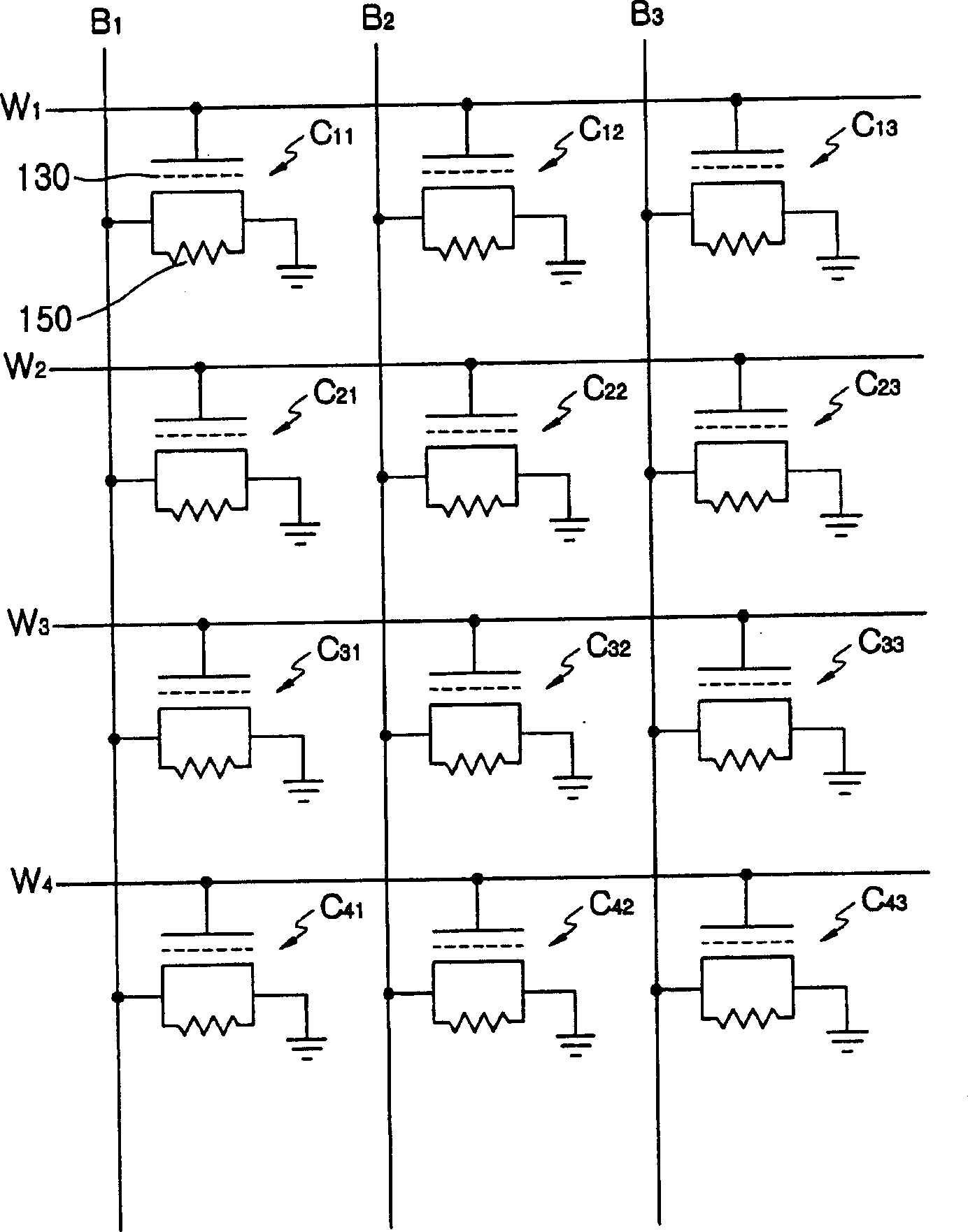
[0025] figure 1 It is a schematic circuit diagram showing a NOR type hybrid multi-bit nonvolatile memory device according to an embodiment of the present invention. refer to figure 1 , the NOR cell array structure includes multiple unit cells C 11 、C 12 、C 13 、C 21 、C 22 、C 23 、C 31 、C 32 and C 33 , all unit cells are arranged in a matrix of rows and columns. figure 1 4×3 unit cells are exemplarily shown, b...


PUM


Abstract

The invention relates to a NOR type hybrid multi-bit nonvolatile memory device and operation method thereof. A hybrid multi-bit memory device may include a plurality of unit cells arranged in a matrix of a plurality of rows and columns. Each of the unit cells may include a first memory unit and a second memory unit. The first and second memory unit may share a source and a drain. The first memory unit of each unit cell arranged in each row may be connected to one of a plurality of word lines, and the drain of each unit cell arranged in each column may be connected to one of a plurality of bit lines.

Description

technical field [0001] The present invention relates to a semiconductor memory device, and more particularly to a multi-bit non-volatile memory (NVM) device and an operating method thereof. Background technique [0002] As the demand for mobile phones and digital cameras increases, the demand for NVM devices is also increasing because of its advantages over DRAM used in computers. NVM devices can process data quickly and store data even when power is no longer provided. [0003] NVM devices are classified into threshold voltage shifting devices, charge displacement devices, and resistance changing devices. According to the type of the storage node, the threshold voltage transition type device is classified into a flash memory device having a floating gate, and a SONOS device having a charge trapping layer. Charge displacement devices are divided into nanocrystalline ferroelectric RAM (FRAM) devices and polymer devices. Resistance change devices are classified into magneti...

Claims


Application Information

Patent Timeline
Patent Type & Authority Applications(China)
IPC IPC(8): H01L27/115H01L29/78
CPCA47G25/0692Y02W30/62
Inventor 金元柱朴允童
Owner SAMSUNG ELECTRONICS CO LTD
Why Eureka
Try Eureka