Driving circuit with low current loss

A technology for driving circuits and level shifting circuits, which is applied in the direction of reducing power consumption, logic circuits, logic circuit coupling/interface using field effect transistors, etc., and can solve problems such as large current consumption

Inactive Publication Date: 2003-09-03
MITSUBISHI ELECTRIC CORP
View PDF0 Cites 6 Cited by
  • Summary
  • Abstract
  • Description
  • Claims
  • Application Information

AI Technical Summary

Problems solved by technology

[0005] However, in the conventional drive circuit 300, since a constant through current always flows from the node of the power supply potential VCC to the node of the ground potential GND through the transistors 301-304 and the constant current source 305, there is a so-called large current consumption problem. question

Method used


Image

  • Driving circuit with low current loss
  • Driving circuit with low current loss
  • Driving circuit with low current loss

Examples


Embodiment 1

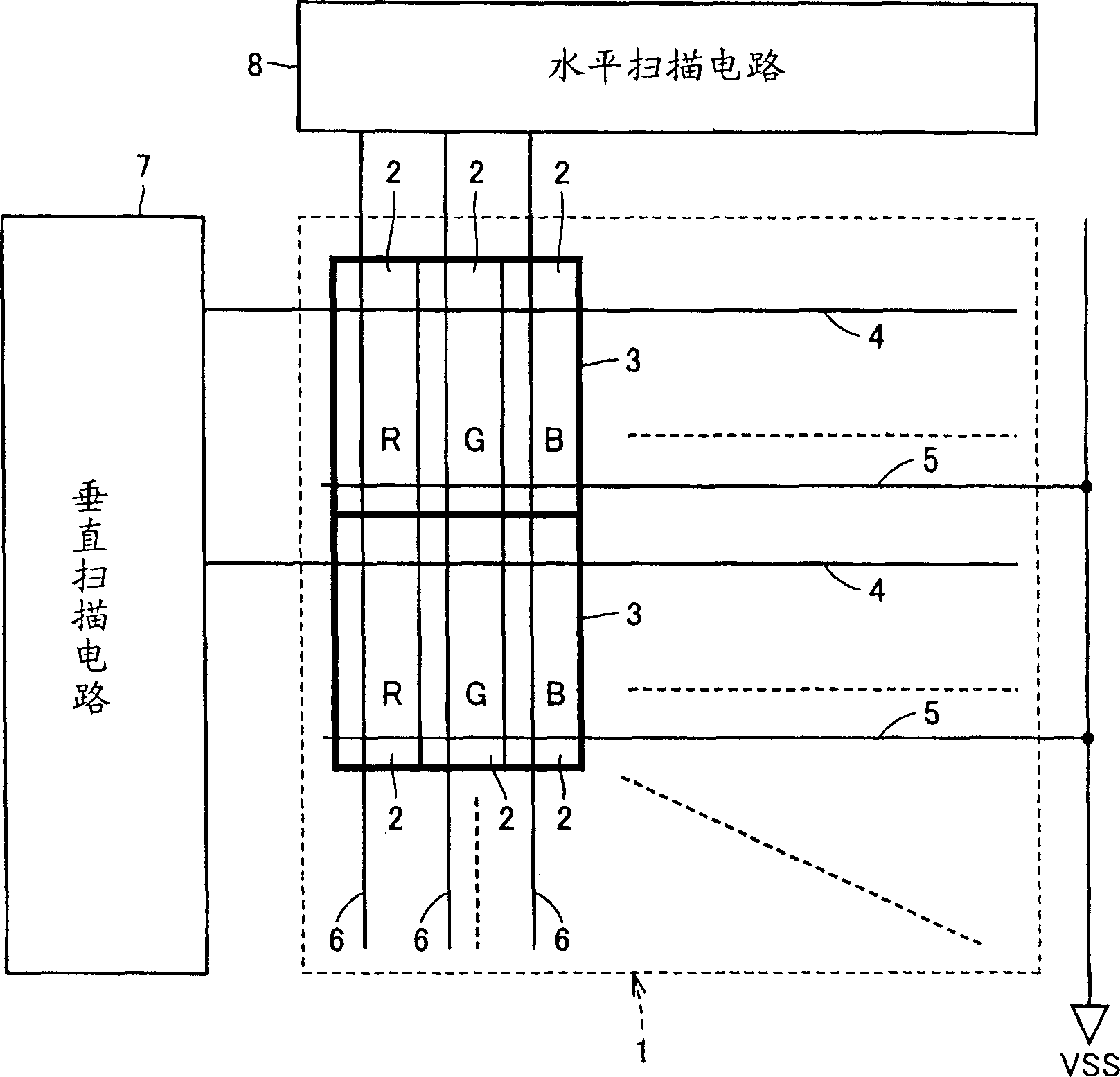
[0092] figure 1 It is a block diagram showing the configuration of the color liquid crystal display device according to Embodiment 1 of the present invention. exist figure 1 Among them, the color liquid crystal display device includes a liquid crystal panel 1, a vertical scanning circuit 7, and a horizontal scanning circuit 8, and is installed in, for example, a mobile phone.

[0093] The liquid crystal panel 1 includes a plurality of liquid crystal cells 2 arranged in multiple rows and columns, scanning lines 4 and common potential lines 5 corresponding to each row, and data lines 6 corresponding to each column.

[0094] The liquid crystal cells 2 are arranged in groups of three in each row. R, G, and B color filters are respectively provided in the three liquid crystal cells 2 of each group. Three liquid crystal cells 2 of each group constitute one pixel 3 .

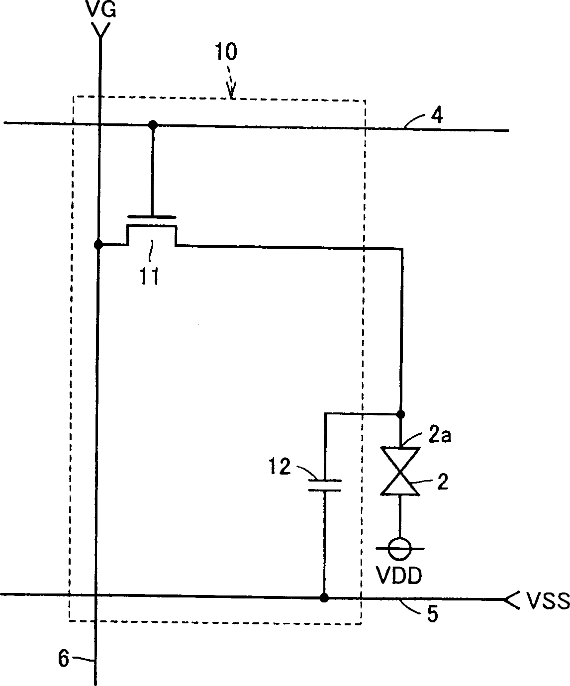
[0095] Such as figure 2 As shown, a liquid drive circuit 10 is provided in each liquid crystal cell 2 . The...

Embodiment 2

[0140] In Example 1, although the threshold voltages of all transistors of the same polarity are assumed to be the same, actually, the threshold voltages of transistors may vary due to fluctuations in manufacturing conditions or the like. VI is not equal to VO if a difference occurs in the threshold voltages of the transistors. In Embodiment 2, this problem can be solved.

[0141] Figure 10 It is a circuit diagram showing the structure of the level shift circuit 40 of the driving circuit of Embodiment 2 of the present invention, and is the same as Figure 4 Figure 21 of the level shift circuit for comparison. refer to Figure 10 , level shift circuit 40 with Figure 4 The difference of the level shift circuit 21 is that the N-type transistors 23 and P Type transistor 24.

[0142] The respective fuses 41.1-41.m are formed of aluminum wiring or the like for connecting transistors to each other. One side electrodes of the fuses 41.1-41.m are all connected to the node N22....

Embodiment 3

[0148] Figure 11 It is a circuit diagram showing the structure of the level shift circuit 45 of the driving circuit of Embodiment 3 of the present invention, and is the same as Figure 4 A diagram of the level shifting circuit 2 5 for comparison. refer to Figure 11 , level shift circuit 45 with Figure 4 The difference of the level shift circuit 25 is that the N-type transistor 26 and the P-type transistor 27 are replaced by fuses 46.1-46.m, N-type transistors 47.0-47.m and P-type transistors 48.0-48.m.

[0149] The respective fuses 46.1-46.m are formed of aluminum wiring or the like for connecting transistors to each other. The electrodes on one side of the fuses 46.1-46.m are all connected to the nodes of the fourth power supply potential V4.

[0150] Set the gate amplitude of N-type transistor 47.0-47.m and Figure 4 The gate amplitudes of the N-type transistors 26 are the same. The drain of the N-type transistor 47.0 is connected to the node of the fourth power suppl...


PUM


Abstract

A drive circuit includes: a first level shift circuit outputting a potential higher than an input potential by a prescribed voltage; a pull-up circuit outputting a potential lower than an output potential of the first level shift circuit by the prescribed voltage to an output node; a second level shift circuit outputting a potential lower than the input potential by the prescribed voltage; a pull-down circuit outputting a potential higher than an output potential of the second level shift circuit by the prescribed voltage to output node; and a capacitor connected between output nodes of the first and second level shift circuits. Accordingly, a through-current is reduced.

Description

technical field [0001] The present invention relates to a driving circuit, and specifically relates to a driving circuit that outputs a potential corresponding to an input potential to an output node. Background technique [0002] Conventionally, a driving circuit for transmitting a potential generated by a potential generating circuit having a low driving capability to a load is provided in a semiconductor integrated circuit device. Figure 80 is a circuit diagram showing the configuration of such a driving circuit 300 . exist Figure 80 Among them, the drive circuit 300 includes P-type field effect transistors (hereinafter referred to as P-type transistors) 301, 302, N-type field effect transistors (hereinafter referred to as N-type transistors) 303, 304 and a constant current source 305. [0003] The P-type transistors 301 and 302 are respectively connected between the node of the power supply potential VCC and the nodes N301 and 302, and their gates are connected to the ...

Claims


Application Information

Patent Timeline
Patent Type & Authority Applications(China)
IPC IPC(8): H03K17/16G09G3/36H03K17/687H03K17/693H03K19/00H03K19/0185
CPCG09G3/3688H03K19/018571G09G2310/0289H03K19/0013G09G3/36
Inventor 飞田洋一
Owner MITSUBISHI ELECTRIC CORP
Why Eureka
Try Eureka