A system and method for testing and configuring semiconductor functional circuits

A configuration method and function technology, applied in the direction of single semiconductor device testing, using configuration testing to detect faulty hardware, semiconductor/solid state device testing/measurement, etc., can solve the problem of available integrated circuits that cannot perform floating-point operations, and does not provide a full range of functions And other issues

Inactive Publication Date: 2006-10-18
NVIDIA CORP
View PDF0 Cites 7 Cited by
  • Summary
  • Abstract
  • Description
  • Claims
  • Application Information

AI Technical Summary

Problems solved by technology

Additionally, the end result is a usable integrated circuit that has limited capabilities and does not provide a full range of functions (eg, cannot perform floating point operations)

Method used


Image

  • A system and method for testing and configuring semiconductor functional circuits
  • A system and method for testing and configuring semiconductor functional circuits
  • A system and method for testing and configuring semiconductor functional circuits

Examples


Embodiment Construction

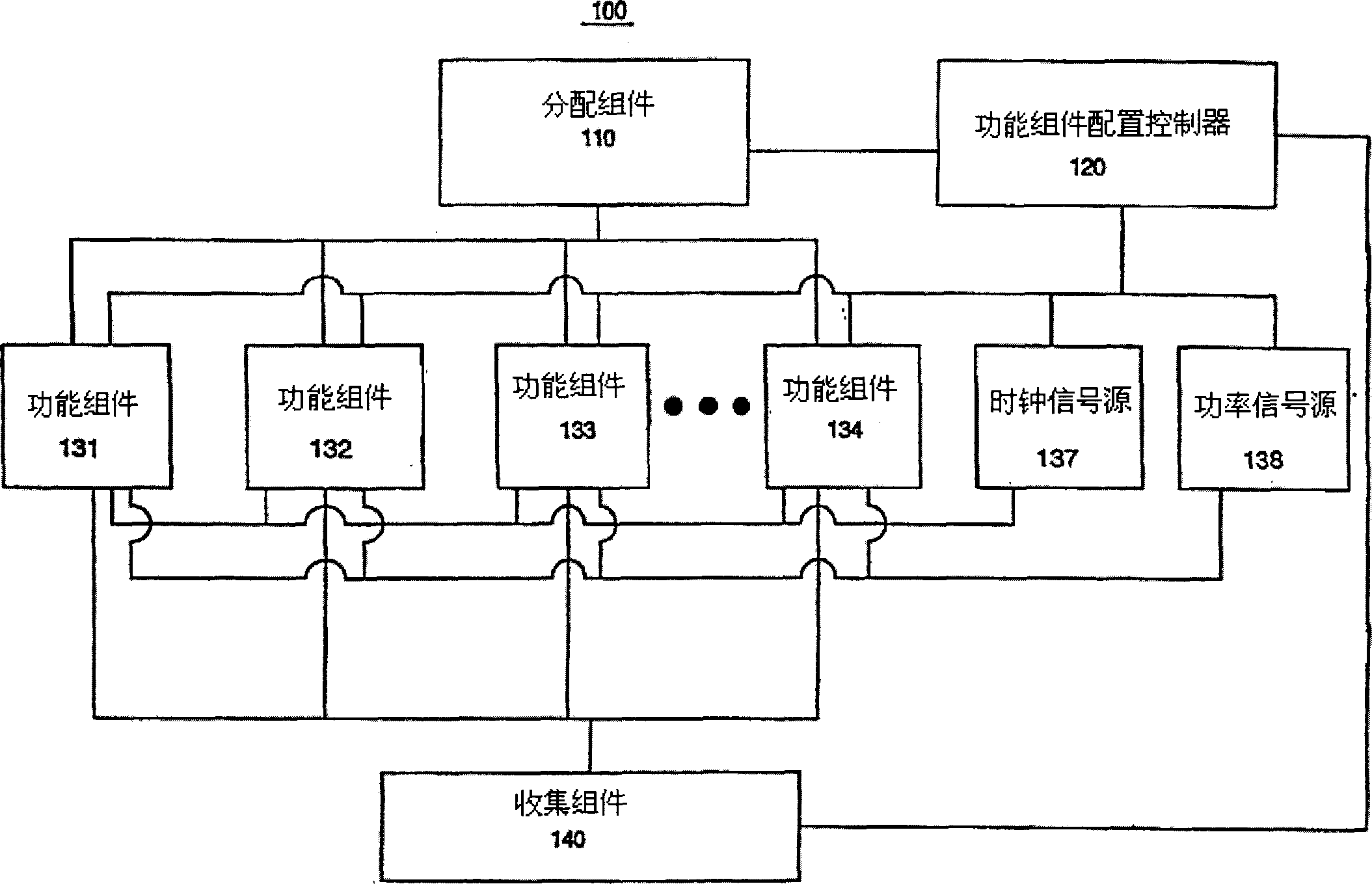
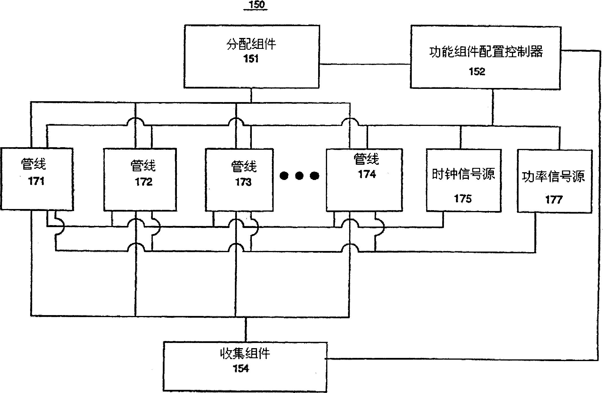
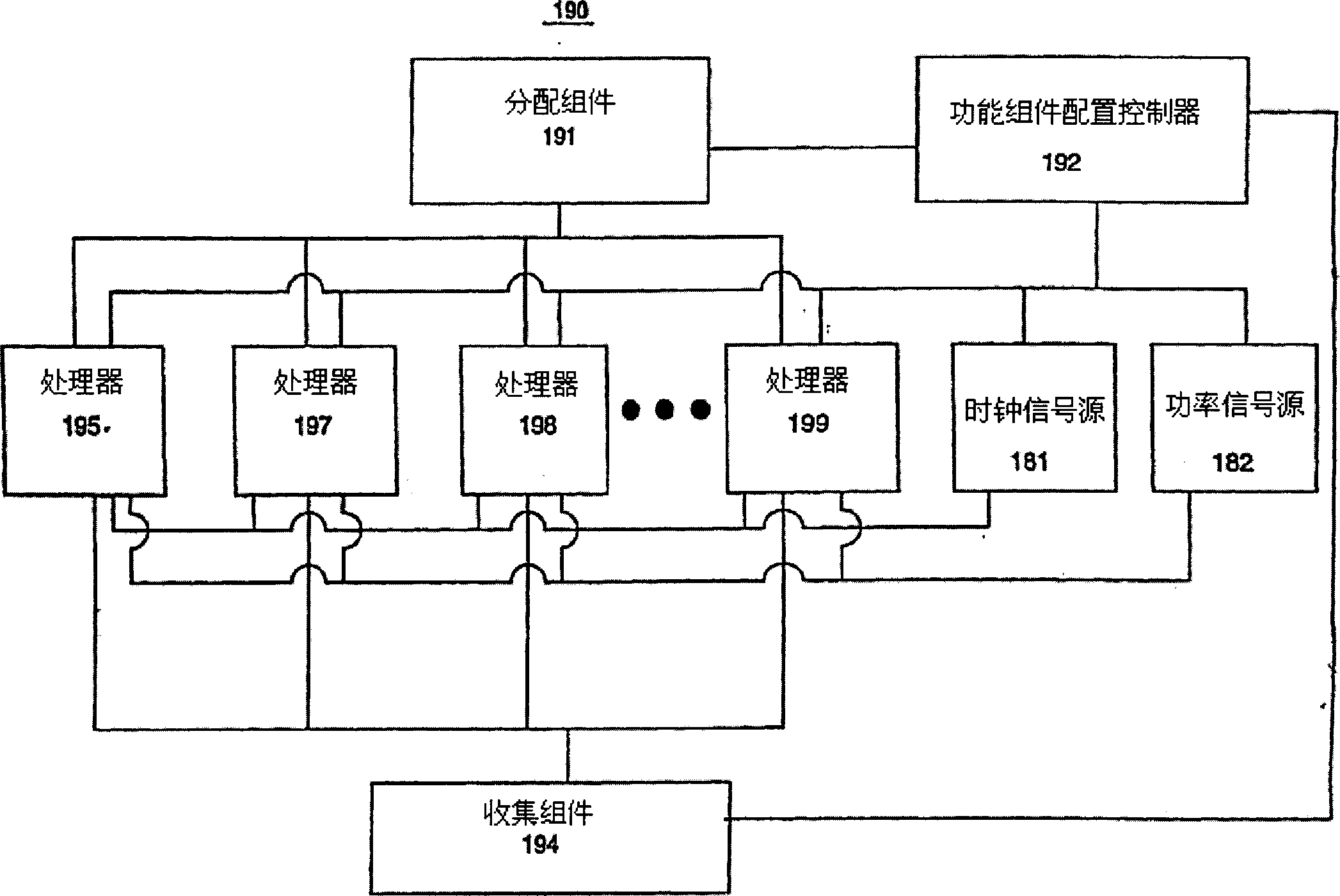
[0034]Reference will now be made in detail to the preferred embodiments of the invention, examples of which are illustrated in the accompanying drawings. While the invention will be described in conjunction with the preferred embodiments, it will be understood that it is not intended to limit the invention to these embodiments. On the contrary, the invention is intended to cover alternatives, modifications and equivalents, which may be included within the spirit and scope of the invention as defined by the appended claims. Furthermore, in the following detailed description of the invention. Numerous specific details are set forth in order to provide a thorough understanding of the invention. It will be apparent, however, to one of ordinary skill in the art that the present invention may be practiced without these specific details. In other instances, well-known methods, procedures, components, and circuits have been described in detail so as not to unnecessarily obscure aspe...


PUM


Abstract

Disclosed here are systems and methods to enable configuration of functional components in integrated circuits. A present invention system and method can flexibly change the operational characteristics of functional components in an integrated circuit die based upon a variety of factors including manufacturing defects, compatibility characteristics, performance requirements, and system health (e.g., the number of components operating properly). Functional component operational behavior is tested and analyzed at various levels of configuration abstraction and component organization (e.g., topological inversion analysis). The testing and analysis can be performed in parallel on numerous functional components. Functional component configuration related information is presented in a graphical user interface (GUI) at various levels of granularity and in real time.; The graphical user interface can facilitate user interaction in recognizing failure patterns, production test tuning and field configuration algorithm adjustment. The testing and analysis information can also be organized in a variety of convenient database formats.

Description

[0001] This patent application asserts co-pending co-ownership of U.S. Patent Application No. 60 / 503,710 filed September 15, 2003, U.S. Patent Application No. 10 / 740,721 filed December 18, 2003, December 2003 U.S. Patent Application No. 10 / 740,722 filed on December 18, 10 / 740,723 filed on December 18, 2003, U.S. Patent Application No. 10 / 740,779 filed on December 18, 2003 and Claim to US Patent Application Serial No. 10 / 876,340, filed June 23, 2004, which is incorporated herein by reference. technical field [0002] The present invention relates to the field of semiconductor manufacturing. In particular, the present invention relates to a system and method for dynamically configuring the operational characteristics of functional components within an integrated circuit. Background technique [0003] Electronic systems and circuits have contributed significantly to the advancement of modern society and are used in numerous applications to achieve beneficial results. Numerous...

Claims


Application Information

Patent Timeline
IPC IPC(8): G06F11/00G01M99/00G01R31/26G01R31/3185G06F11/267G06F17/50G06F19/00G09G5/02H01L21/66
CPCG01R31/31704G01R31/3185G01R31/318544G01R31/318566G06F11/22G06F11/2289G06F11/267
Inventor 迈克尔·B·戴蒙德约翰·S·蒙特赖姆詹姆斯·M·范戴克迈克尔·B·纳吉肖恩·J·特赖希勒
Owner NVIDIA CORP
Why Eureka
Try Eureka