Non-volatile memory, its production and operation
A non-volatile storage, non-volatile technology, applied in semiconductor/solid-state device manufacturing, electric solid-state devices, semiconductor devices, etc., can solve the problem of the inability to effectively improve the integration of components, achieve high electron injection efficiency, and improve integration. , the effect of reducing power loss
- Summary
- Abstract
- Description
- Claims
- Application Information
AI Technical Summary
Problems solved by technology
Method used
Image

Examples
Embodiment Construction
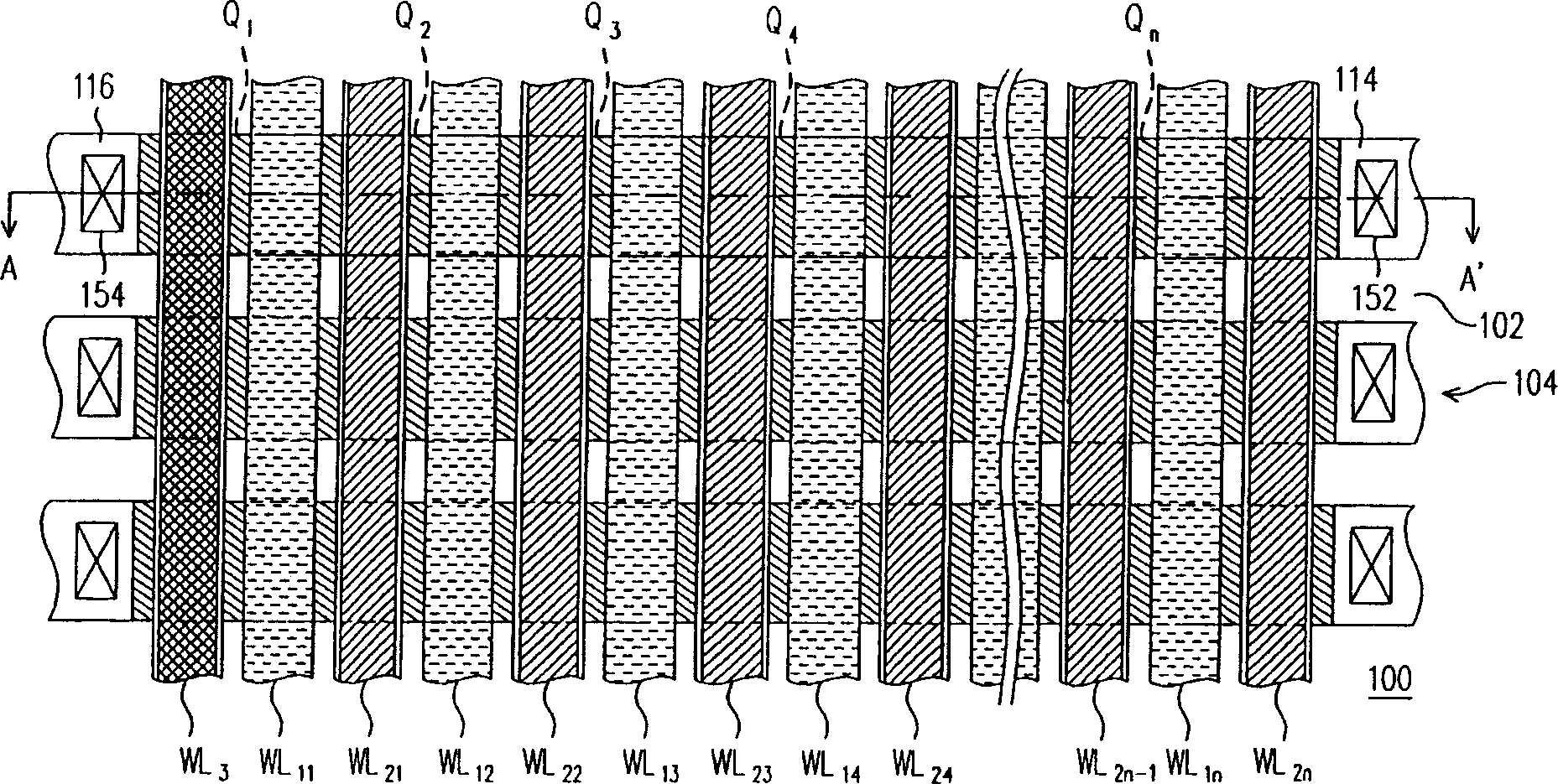
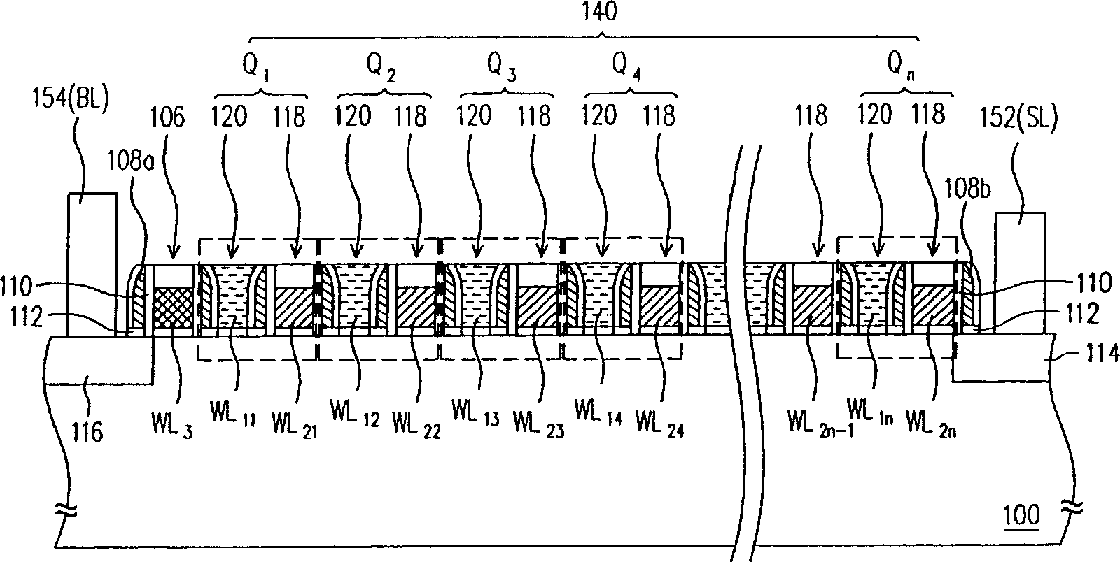
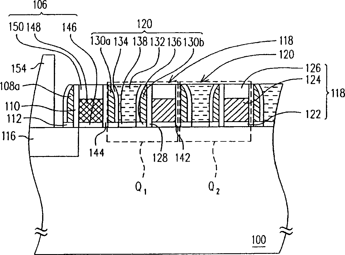
[0065] Figure 1A It is a top view showing the non-volatile memory of the present invention. Figure 1B for illustration Figure 1A Structural cross-section along line A-A'. Figure 1C It is a cross-sectional view showing the structure of the memory unit and the switch unit of the present invention.
[0066] Please also refer to Figure 1A , Figure 1B and Figure 1C , the non-volatile memory structure of the present invention is at least composed of a substrate 100, an element isolation structure 102, an active region 104, a plurality of memory cells Q1-Qn, a switch unit 106, conductor spacers 108a, 108b, an insulating layer 110, and a gate interlayer. The electrical layer 112 , the source region 114 and the drain region 116 are formed.
[0067] The substrate 100 is, for example, a silicon substrate, and the substrate 100 can be a P-type substrate or an N-type substrate. The device isolation structure 102 is disposed in the substrate 100 to define an active region 104 . ...
PUM
 Abstract
Description
Claims
Application Information