Mems switch

A switch and conductive layer technology, applied in the field of MEMS switches, can solve the problems of high driving voltage, low operating speed, and insufficient reliability.

Inactive Publication Date: 2006-12-06
PANASONIC CORP
View PDF2 Cites 7 Cited by
  • Summary
  • Abstract
  • Description
  • Claims
  • Application Information

AI Technical Summary

Problems solved by technology

However, there is a problem in that MEMS switches are hindered from being put into practical use due to their high driving voltage, low operating speed, insufficient reliability, etc.
Therefore, there is a problem that the capacitance change rate decreases

Method used


Image

  • Mems switch
  • Mems switch
  • Mems switch

Examples


Embodiment 1

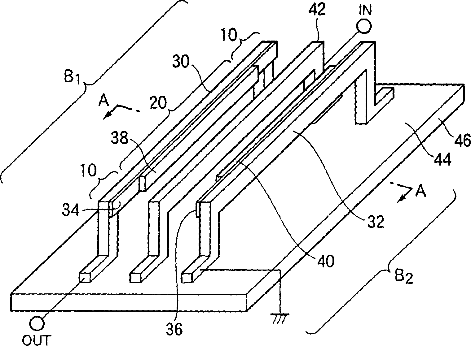
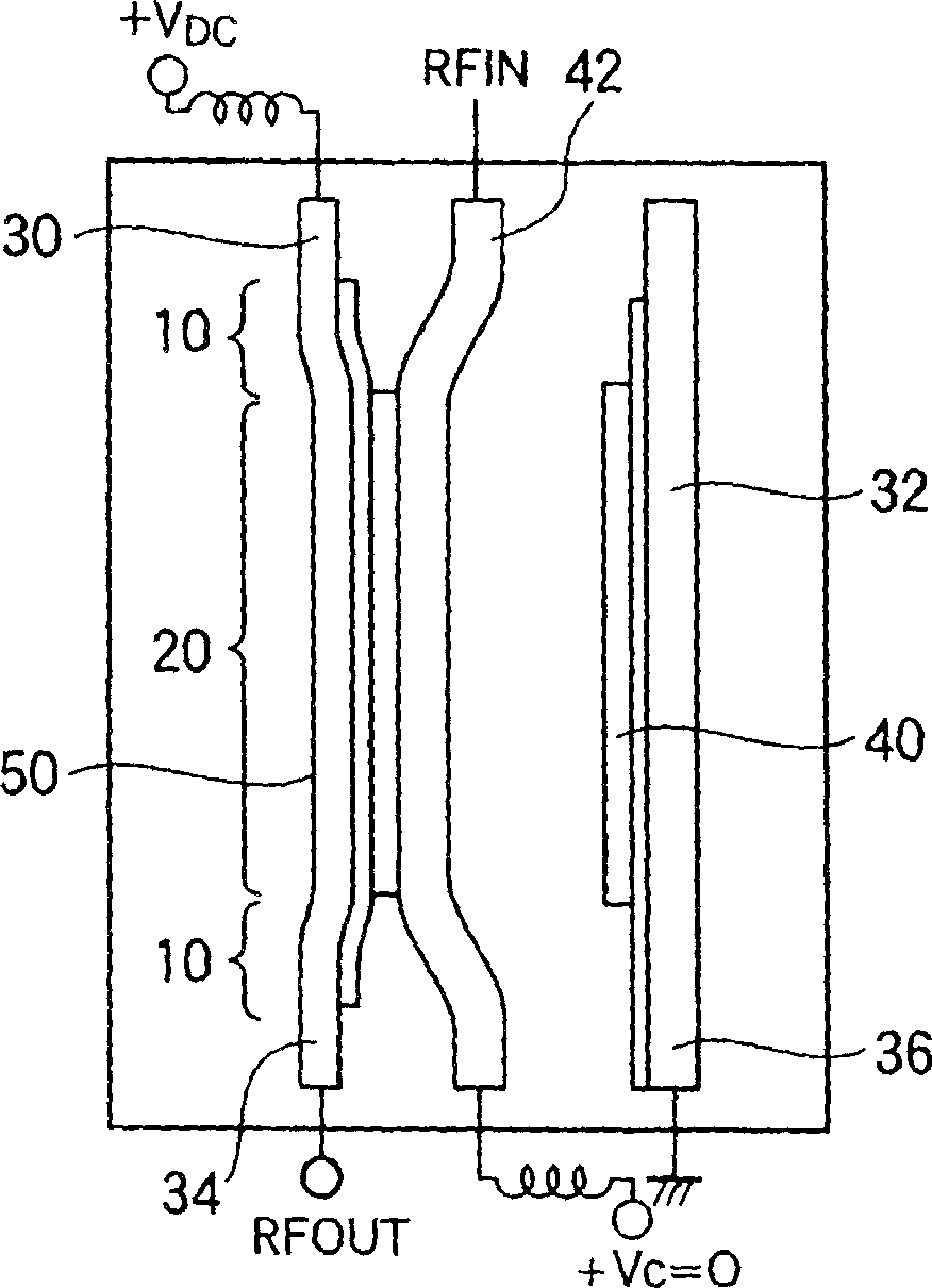
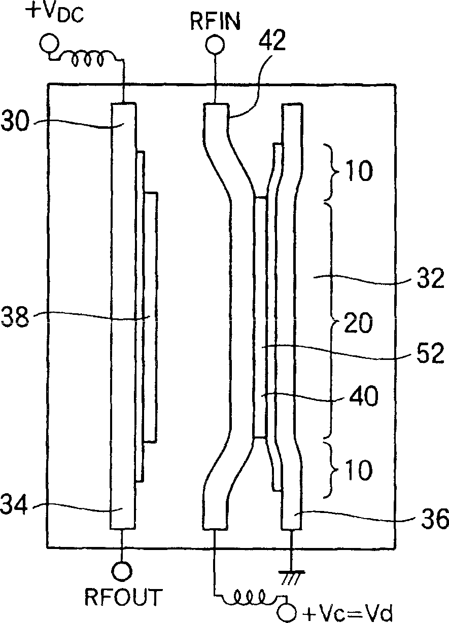
[0110] The MEMS switch is formed by processing the silicon substrate 1 with MEMS technology. like figure 1 As shown, the MEMS is formed such that air bridges are disposed in the surface of the silicon substrate 46 . The MEMS switch is formed by a conductive beam 42 and first and second three-layer structure beams B1 and B2 each having a capacitive structure. The conductive beam 42 and the three-layer structure beam B1 are respectively connected to the input terminal and the output terminal, and the three-layer structure beam B2 is also grounded. Each of these first and second three-layer structural beams is formed by sandwiching a dielectric layer between a first conductive layer 38 , 40 and a second conductive layer 30 , 32 . Then, the first and second three-layer structure beams B1 and B2 having the conductive beam 42 interposed therebetween are displaced on a plane parallel to the substrate due to electrostatic force, so that the conductive beam 42 and the first conductiv...

Embodiment 2

[0145] The driving method and basic configuration of the MEMS switch according to this embodiment 2 are similar to those in embodiment 1. All beams were formed as arched beams in Example 1. However, if Figure 10 As shown, the MEMS switch according to Embodiment 2 is characterized in that the centrally located conductive beam 42 is formed to have a cantilever beam structure slightly shorter than the arched beam. That is, if Figure 10 As shown, the MEMS switch is characterized in that the conductive beam 42 is fabricated to be half the length of any other beam, ie 250 μm.

[0146] The MEMS switch according to this embodiment differs from the MEMS switch according to Embodiment 1 in that the second conductive layer forming the second three-layer structural beam is not grounded but connected to the second output terminal.

[0147] With this configuration, when the conductive beam 42 is adjacent to the first three-layer structural beam and the second three-layer structural bea...

Embodiment 3

[0160] According to this example, as Figure 12 As shown, protruding portions serving as capacitive regions 84 and drive surfaces 86 are formed in the surfaces of the second conductive layers 30 and 32 . Figure 12 shows the as-of status. In the conducting state, the conductive beam 42 adjoins the metal-to-metal contact surface 82 of each capacitive region, resulting in electrical coupling.

[0161] Next, the coupling state in the on state will be explained. Figure 14 is an enlarged view showing the contact surface in the conduction state. A state is shown in which the conductive beam 42 is adjacent to the first conductive layer (first electrode) 38 of the first three-layer structure beam. When the conductive beam 42 and the metal-metal contact surface 82 move to abut each other due to electrostatic force, the potential of the first conductive layer 38 forming the first three-layer structure beam becomes equal to the potential of the conductive beam 42 . Thus, a capacitor...


PUM


Abstract

A fine MEMS switch easily producible and exhibiting an adequate IN/OFF capacitance variation ratio. The MEMS switch comprises a substrate (46), a conductive beam(42) formed on the substrate, and three-layer structure beams (B1, B2) formed on the substrate and opposed to the conductive beam. The MEMS switch is characterized in that the three-layer structure beams include first conductive layers (38, 40), second conductive layers (30, 32), and dielectric layers (34, 36) interposed between the respective first and second conductive layers, the first conductive layers are opposed to the conductive beam (42), at least one of the conductive beam (42) and the three-layer structure beams is deformed by the electric static force in a plane parallel to the substrate (46) thereby to bring the conductive beam (42) and the first electrode (38, 40) into contact with each other, and a conduction path between the conductive beam (42) and the second conductive layer (30, 32) is formed when the conductive beam (42) and the first conductive layer are in contact with each other.

Description

technical field [0001] The present invention relates to microelectromechanical systems (MEMS) switches, and in particular to MEMS switches formed by MEMS or nanoelectromechanical technology (NEMS) technology. Background technique [0002] Due to the desire for electromechanical switches such as MEMS switches to have better properties than GaAS FET switches or PIN-type diode switches, extensive research has been conducted to apply MEMS switches to wireless communication systems. Previously, MEMS attracted people's attention because of its low loss, good isolation, low power consumption, good linearity, miniaturization and high integration capabilities. However, there are problems in that MEMS switches are hindered from being put into practical use due to their high driving voltage, low operating speed, insufficient reliability, and the like. [0003] Generally, a capacitively coupled MEMS switch is constituted by a fixed electrode, a moving electrode disposed relative to the...

Claims


Application Information

Patent Timeline
Patent Type & Authority Applications(China)
IPC IPC(8): H01H59/00
Inventor 桥村昭范内藤康幸中村邦彦中西淑人
Owner PANASONIC CORP
Why Eureka
Try Eureka