

Solid-state image sensing device and method for fabricating the same
A technology for a solid-state imaging device and a manufacturing method, which is applied in the manufacture of semiconductor/solid-state devices, electric solid-state devices, radiation control devices, etc., can solve the problems of miniaturization limitations and other problems, and achieve the effect of reducing manufacturing costs.
- Summary
- Abstract
- Description
- Claims
- Application Information
AI Technical Summary
Problems solved by technology
Method used
Image

Examples
no. 1 approach
[0080] Hereinafter, the solid-state imaging device and its manufacturing method according to the first embodiment of the present invention will be described with reference to the drawings. In addition, each drawing shows the state after dicing a wafer (wafer) into a solid-state imaging device (chip) unless otherwise specified.
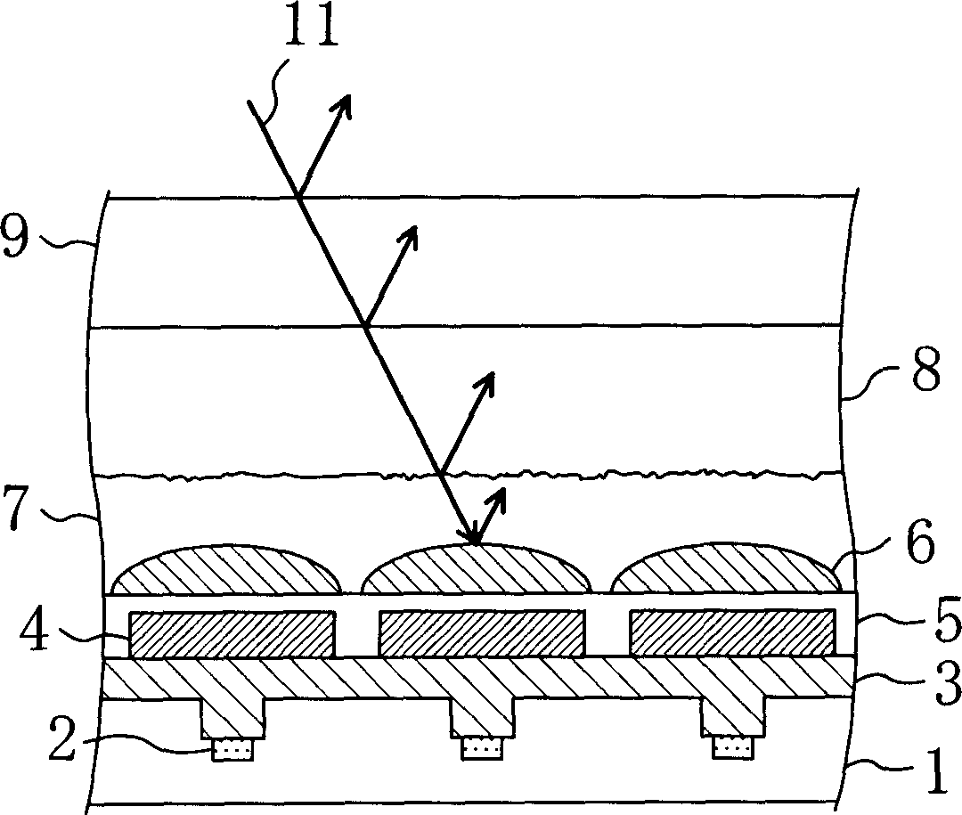
[0081] figure 1 , is a cross-sectional view of the solid-state imaging device according to the first embodiment of the present invention. Yet, figure 1 In , the appearance of light incident on the microlens of the solid-state imaging device according to the present embodiment is also shown together.
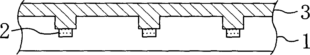
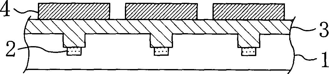
[0082] Such as figure 1 As shown, a photodiode 2 for converting incident light into an electrical signal is provided on the bottom of a recess provided for each pixel on the surface of a charge junction device (CCD) type solid-state imaging device substrate 1 . On the substrate 1 for a solid-state imaging device, a first acrylic smoothing film 3 fo...
no. 2 approach
[0119] Hereinafter, a solid-state imaging device and a manufacturing method thereof according to a second embodiment of the present invention will be described with reference to the drawings. The biggest difference between the second embodiment and the first embodiment is that before the formation of the resin layer, a spacer is provided around the light receiving area (pixel area) to define the thickness of the resin layer. This facilitates regulation of the thickness of the fluorine-containing element resin material layer, that is, the resin layer serving as the adhesive layer between the semiconductor substrate and the transparent substrate.
[0120] Figure 7(a) to Figure 7(f) 8( a ) to FIG. 8( d ), each step of the method of manufacturing the solid-state imaging device according to this embodiment is shown. Shang, in Figure 7(a) to Figure 7(f) and Figure 8(a) to Figure 8(d), and figure 1 and Figure 2(a) to Figure 2(f) Components that are the same as those of the so...
PUM
| Property | Measurement | Unit |
|---|---|---|
| Thickness | aaaaa | aaaaa |
| Thickness | aaaaa | aaaaa |
Abstract
Description
Claims
Application Information