Printing circuit board with modified power zone block

A technology of printed circuit boards and multi-layer circuit boards, applied in the directions of printed circuits, printed circuits, printed circuit components, etc., can solve the problem of reducing the service life of printed circuit boards, generating heat, and destroying the integrity and stability of the power layer and ground layer. and other problems to achieve the effect of improving integrity, increasing service life and improving quality

Inactive Publication Date: 2007-01-24
HONG FU JIN PRECISION IND (SHENZHEN) CO LTD +1
View PDF0 Cites 3 Cited by
  • Summary
  • Abstract
  • Description
  • Claims
  • Application Information

AI Technical Summary

Problems solved by technology

Such vias have current passing through them, causing self-heating and reducing the service life of the printed circuit board. At the same time, because such vias always run through the dual power supply block and the ground layer therebetween, a large number of such vias also Seriously compromise the integrity and stability of the power and ground planes

Method used


Image

  • Printing circuit board with modified power zone block
  • Printing circuit board with modified power zone block
  • Printing circuit board with modified power zone block

Examples


Embodiment Construction

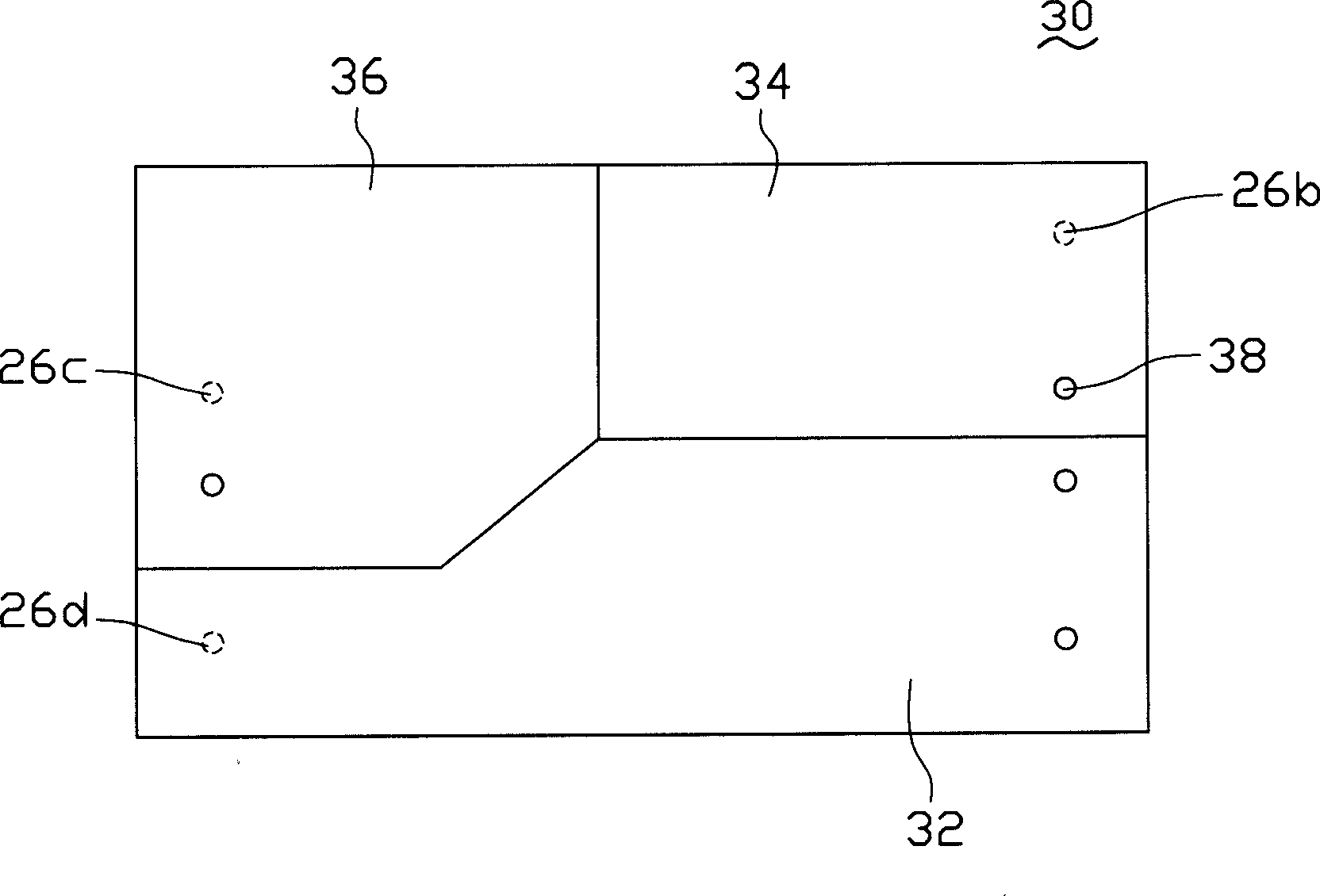
[0016] see Figure 4, a preferred embodiment of the present invention has a printed circuit board with an improved power supply block, the printed circuit board is a multilayer circuit board, which has a number of component contacts 40, a first power supply block 42, a second power supply block 44 and Several via holes 46 . The component contacts 40 are used to place a large current component (not shown); the first power supply block 42 and the second power supply block 44 are used to jointly provide the high current components installed on the component contacts 40 Working voltage and working current; the via hole 46 runs through and electrically connects the first power supply block 42 and the second power supply block 44 to keep the same voltage. The first power supply block 42 and the second power supply block 44 are all identical in purpose and property, and are located in different layers of the printed circuit board. When the multilayer printed circuit board is a four...


PUM


Abstract

This invention provides a multilayer PCB with improved supply blocks, which has several element contacts, a first supply block, a second supply block and several through holes, in which, said element contacts are used in setting a large current electronic element, said through holes pass through said first supply block, the second block and connect them to keep the voltage of them the same, and the shape of them is the same or similar, which can reduce numbers of the through holes.

Description

【Technical field】 [0001] The invention relates to a printed circuit board, in particular to a printed circuit board with an improved power block. 【Background technique】 [0002] Generally speaking, printed circuit boards have been widely used to assist in the electrical connection between various electronic components, so as to facilitate the transmission of signals between the various electronic components. In the past, the printed circuit board was a single-layer board with only one signal layer on its surface, and the traces on the signal layer were used to connect all the electronic components arranged on the printed circuit board, that is, the traces were used to transmit the Input or output signals of electronic components. When there are multiple different signals between the electronic components, the signal layer requires a complex trace layout to smoothly transmit huge signals between the electronic components, but the printed circuit board itself has area limitat...

Claims


Application Information

Patent Timeline
Patent Type & Authority Applications(China)
IPC IPC(8): H05K1/16H05K1/11
CPCH05K2201/0979H05K1/115H05K2201/093H05K1/0265
Inventor 林有旭叶尚苍黄肇振李传兵
Owner HONG FU JIN PRECISION IND (SHENZHEN) CO LTD
Why Eureka
Try Eureka