Display driver circuit
一种显示驱动、电路的技术,应用在峰值电流抑制领域,能够解决误动作等问题,达到消除误动作、抑制电源电压的变动、峰值电流减小的效果
- Summary
- Abstract
- Description
- Claims
- Application Information
AI Technical Summary
Problems solved by technology
Method used
Image
Examples
Embodiment 1
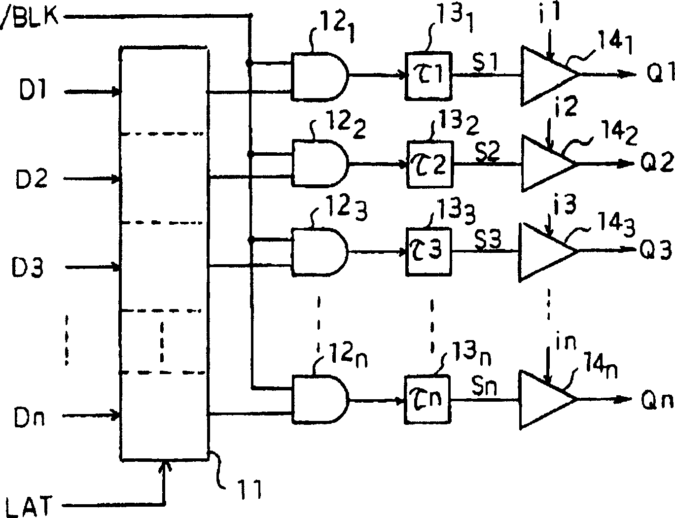
[0021] figure 1 It is a configuration diagram showing the display drive circuit of the first embodiment of the present invention.
[0022] The display drive circuit is a display drive circuit that drives a fluorescent display tube or a liquid crystal display, and has a holding circuit (for example, a data latch) 11, and takes in n display data D1, D2, and D2 provided in parallel in accordance with a latch signal LAT. ..Dn. When the latch signal LAT is'H', the data latch 11 fetches and outputs the display data D1 to Dn in parallel. When the latch signal LAT is'L', it keeps the data fetched during the'H' period as it is. Signal, and continue to output.
[0023] The output side of the data latch 11 and the AND gate 12 gated by the common blank signal / BLK 1 , 12 2 ,...12 n connection. That is, AND gate 12 1 ~12 n When the blank signal / BLK is'L', regardless of the output of the data latch 11, always output'L'. When the blank signal / BLK is'H', the output signal of the data latch 11...
Embodiment 2
[0042] Figure 4 It is a structural diagram showing a display drive circuit of the second embodiment of the present invention. Right and figure 1 The same elements in the elements are given the same symbols.
[0043] The display drive circuit is removed figure 1 Delay circuit in 13 1 ~13 n , Make AND gate 12 1 ~12 n Output side and driver 14 1 ~14 n At the same time, the delay buffer 15 with the same structure as the cascade connection circuit is used. 1 , 15 2 ,...15 n-1 The delay circuit is constructed so that the AND gate 12 1 ~12 n The blank signal / BLK is delayed in sequence. That is, for AND gate 12 1 Apply blank signal / BLK. To AND gate 12 2 Apply using delay buffer 15 1 Delay the blank signal / BLK signal after time τ. To AND gate 12 3 Apply using delay buffer 15 1 And 15 2 Delay the blank signal / BLK signal after the time 2τ. The following is the same, for the final AND gate 12 n Apply using delay buffer 15 1 ~15 n-1 Delay the blank signal / BLK by a time (n-1)τ. The rest of...
Embodiment 3
[0056] Figure 5 It is a diagram showing the structure of a delay buffer according to the third embodiment of the present invention.
[0057] The delay buffer is to replace image 3 Delay buffer 15 1 ~15 n-1 The circuit set up is basically a cascade-connected circuit with two-stage inverters. The front-stage inverter connects two inverters in parallel, and uses a control signal to separate one of the inverters, thereby controlling the delay time.
[0058]That is, the delay buffer has a first CMOS inverter composed of PMOS (P-channel MOS transistors) 21 and 22 connected in series between the power supply potential VDD and the node N1, and connected in series between the node N1 and the ground. NMOS (N-channel MOS transistors) 23 and 24 are formed between the potential GND. The control signal CON and the control signal / CON in which the control signal CON is inverted by the inverter 25 are respectively applied to the gates of the NMOS 24 and PMOS 21 for switching. In addition, a del...
PUM
 Abstract
Description
Claims
Application Information


