Memory device and dual port static RAM

A static random access and memory technology, applied in static memory, digital memory information, information storage, etc., can solve problems such as component performance that has to be considered

Active Publication Date: 2007-01-31
TAIWAN SEMICON MFG CO LTD
View PDF0 Cites 13 Cited by
  • Summary
  • Abstract
  • Description
  • Claims
  • Application Information

AI Technical Summary

Problems solved by technology

Therefore, for cost considerations, a more aggressive layout is often r

Method used


Image

  • Memory device and dual port static RAM
  • Memory device and dual port static RAM
  • Memory device and dual port static RAM

Examples


Embodiment Construction

[0027] In order to make the above-mentioned purposes, features and advantages of the present invention more obvious and understandable, a preferred embodiment is specifically cited below, and in conjunction with the accompanying drawings, the detailed description is as follows:

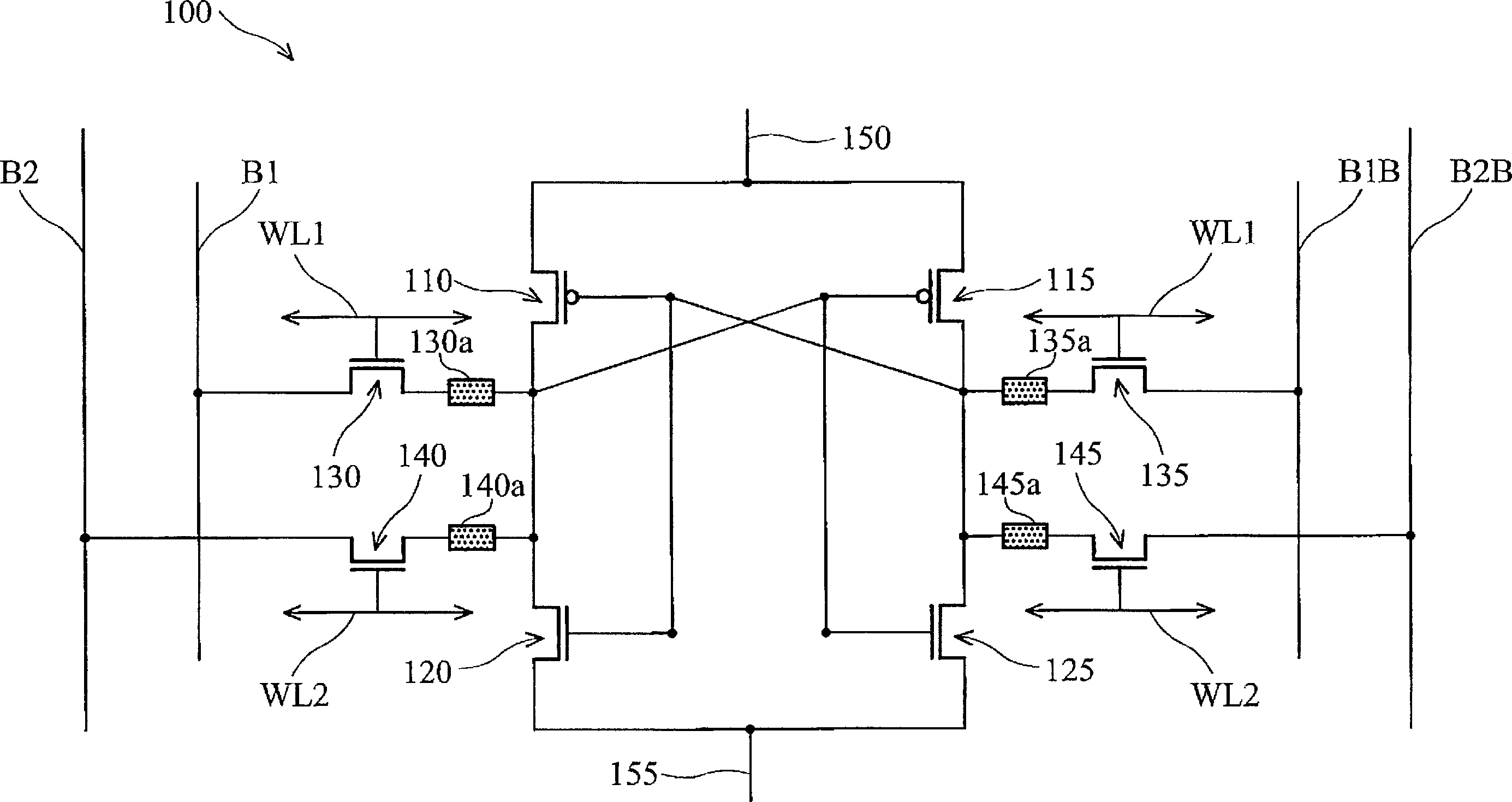
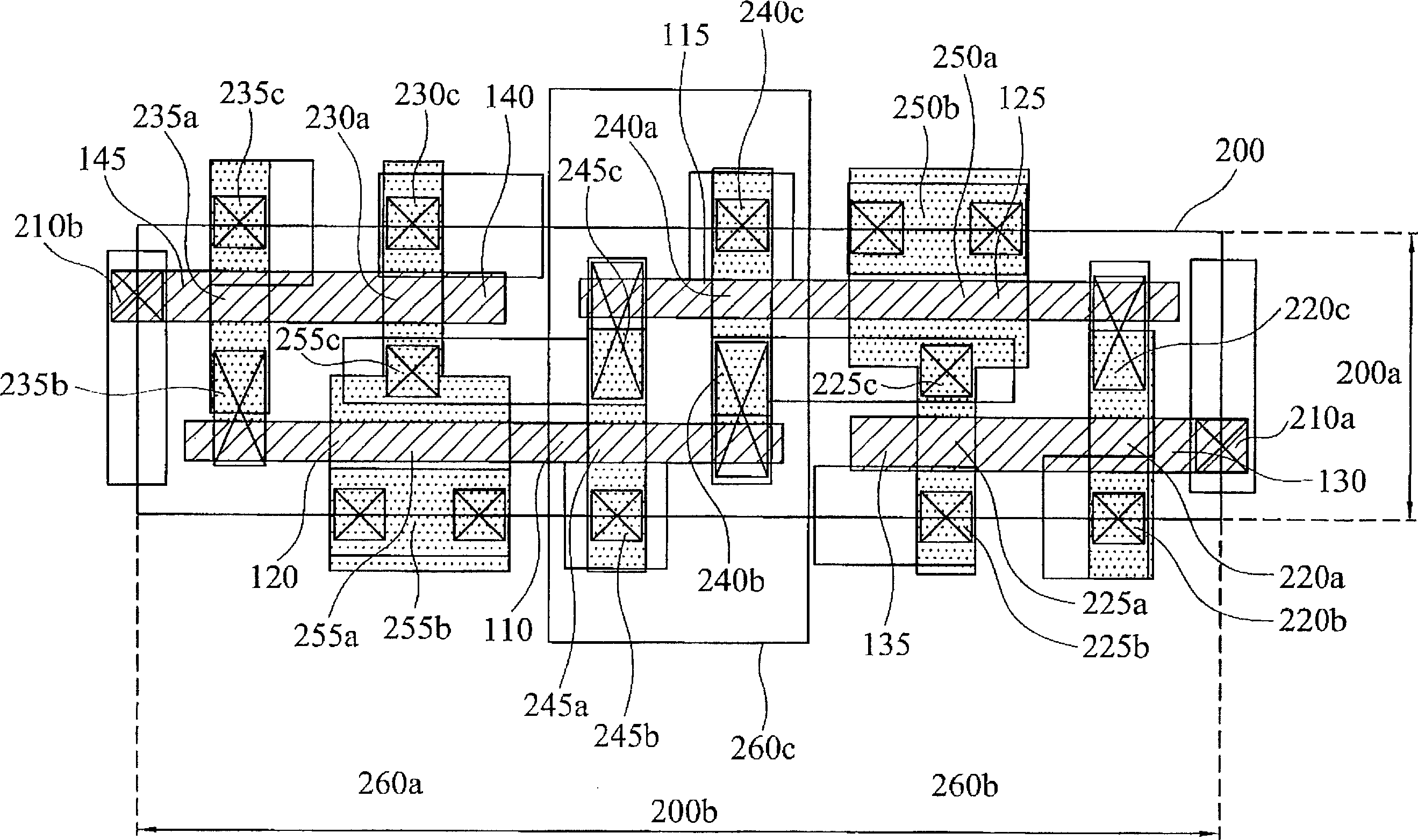
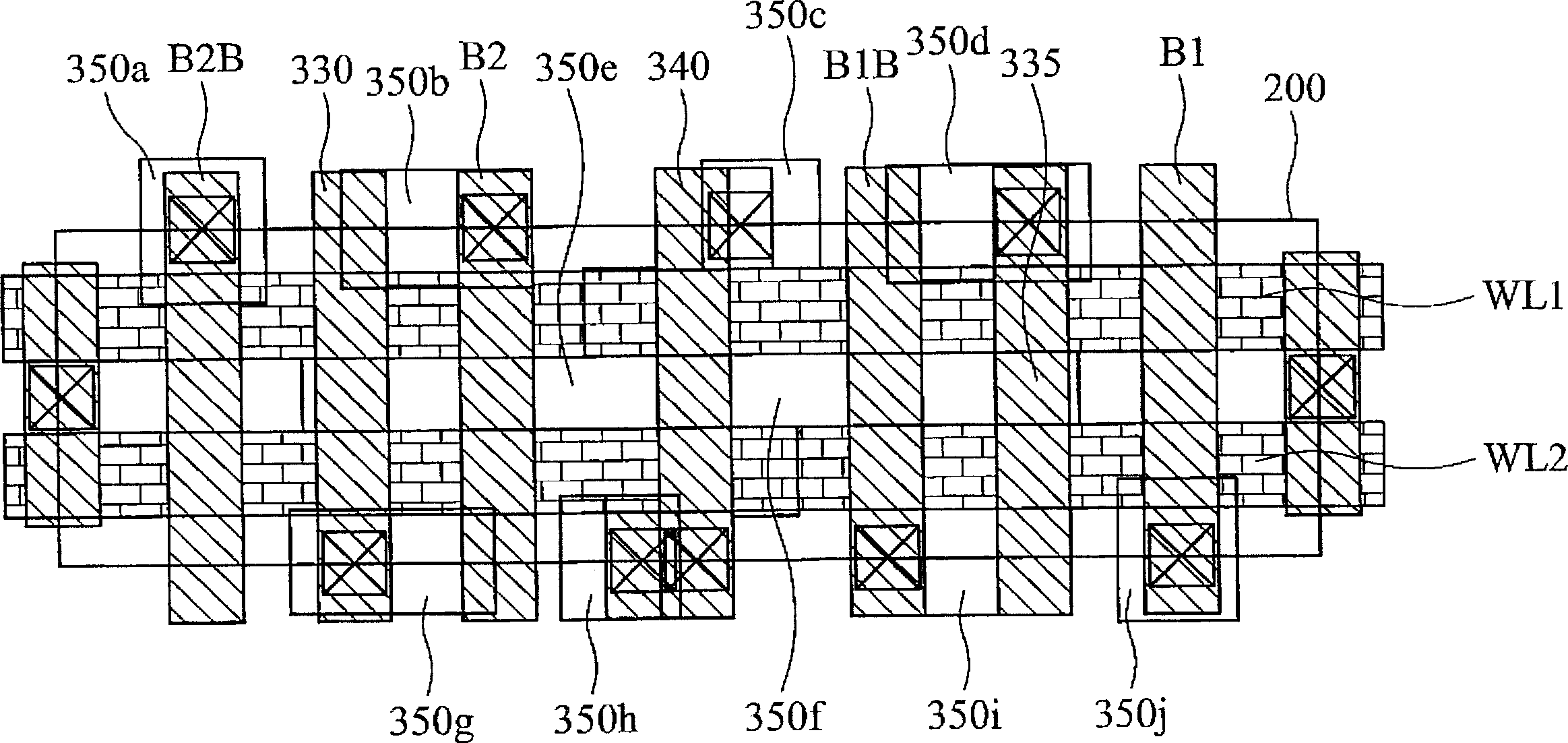
[0028] figure 1 A circuit diagram of a memory is shown. This circuit diagram is a circuit embodiment of a dual-port SRAM cell with eight transistors, denoted by symbol 100 . These eight transistors constitute two interlocked complementary metal-oxide-semiconductor field effect transistors (complementary metal-oxide-semiconductor field effect transistors, CMOSFET) inverters (inverters), and four transfer gate (passgate) transistors ( It is also called pass transistor, access transistor, active transistor). Cell 100 has pull-up transistors 110 and 115 , and pull-down transistors 120 and 125 , as well as pass-gate transistors 130 , 135 , 140 and 145 . In this specification, the pull-up transistor may ...


PUM


Abstract

Disclosed is a memory device and dual port static RAM. The memory device comprises a memory cell arrays, at least two signal lines and a interleaving region. The memory cell arrays comprise a plurality of memorizers arranged in lines or in rows wherein each line or row is provided with several memorizers. The signal lines extend along one line of the memorizers, and are electrically connected with the first end and the second end of each memorizers. The interleaving region is associated with each line, and the second signal line in the first line crosses the first interleaving region. The memory device and dual port static RAM according to the invention can reduce the resistance difference and circuit area, improve the efficiency and mass production.

Description

technical field [0001] The present invention relates generally to semiconductor memory devices, and more particularly to memory devices and dual-port SRAMs with reduced resistance variation. Background technique [0002] The physical size of a feature on a semiconductor chip is generally referred to as the feature size. As long as the feature size is reduced or reduced, more elements or structures can be allowed to be placed on a single wafer, and more elements or structures can be allowed to be placed on a single wafer, thereby reducing the cost per die. round or production cost per wafer. Some semiconductor devices have memory cells, and feature sizes must be reduced to reduce production costs. In addition to reducing the feature size, the level of integration can be increased by changing the layout, allowing more units to be placed on each wafer. Similarly, there are many goals that can be achieved by changing the layout, for example, to improve the performance of the ...

Claims


Application Information

Patent Timeline
IPC IPC(8): G11C11/41G11C11/413
CPCH01L27/1104G11C11/412H01L27/11G11C8/16G11C5/063H10B10/00H10B10/12
Inventor 廖忠志
Owner TAIWAN SEMICON MFG CO LTD
Why Eureka
Try Eureka