Nitride-based compound semiconductor light emitting device and method of fabricating the same
What is Al technical title?
Al technical title is built by PatSnap Al team. It summarizes the technical point description of the patent document.
A light-emitting device and compound technology, applied in the direction of semiconductor lasers, semiconductor devices, lasers, etc., can solve problems such as difficult to form ohmic contacts, and achieve the effect of improving ohmic contact characteristics
Inactive Publication Date: 2007-01-31
SAMSUNG ELECTRONICS CO LTD
View PDF0 Cites 7 Cited by
Summary
Abstract
Description
Claims
Application Information
AI Technical Summary
This helps you quickly interpret patents by identifying the three key elements:
Problems solved by technology
Method used
Benefits of technology
Problems solved by technology
As mentioned above, another disadvantage of Al-Ti based materials is that it can only form ohmic contacts on the Ga pole surface
Al-Ti-based materials are known to be difficult to form ohmic contacts on the N pole surface
Method used
Image
Click on the blue label to locate the original text in one second.
Reading with bidirectional positioning of images and text.
Examples
Embodiment Construction
[0021] A nitride-based compound semiconductor light emitting device and a manufacturing method thereof according to embodiments of the present invention will now be described in detail with reference to the accompanying drawings. In the drawings, the thicknesses of layers and regions are exaggerated for clarity.
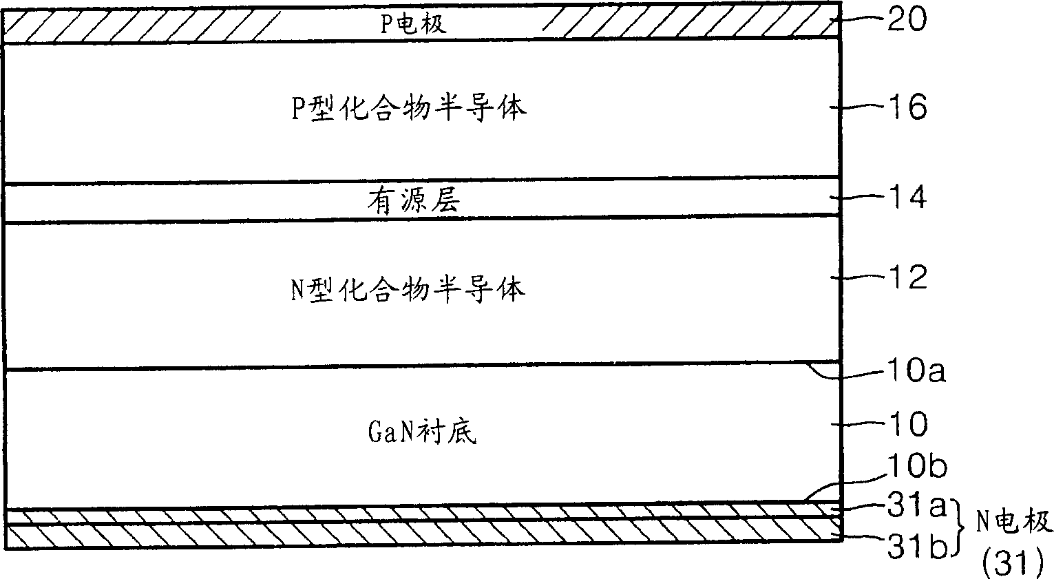
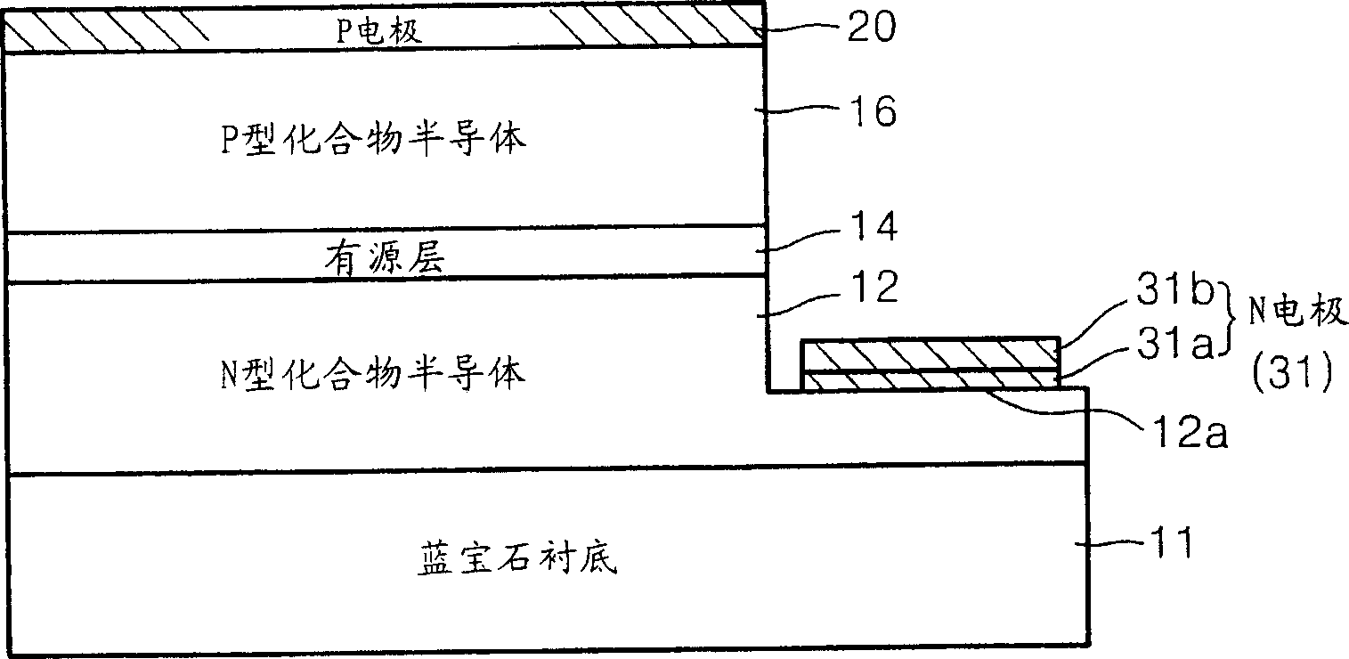
[0022] figure 1 is a schematic cross-sectional view of a nitride-based compound semiconductor light emitting device according to an embodiment of the present invention. refer to figure 1 , the nitride-based compound semiconductor light-emitting device according to the current embodiment of the present invention includes an n-electrode 31, a p-electrode 20, and an n-type compound semiconductor layer 12 formed between the n-electrode 31 and the p-electrode 20, an active layer 14, and a p-electrode type compound semiconductor layer 16. More specifically, n-type compound semiconductor layer 12 , active layer 14 , p-type compound semiconductor layer 16 , and p-electrod...
PUM
Abstract
The invention discloses a nitride-based semiconductor light-emitting device with improved ohmic contact characteristics for an n-electrode and a manufacturing method thereof. The nitride-based semiconductor light emitting device includes an n-electrode, a p-electrode, and an n-type compound semiconductor layer, an active layer, and a p-type semiconductor layer formed between the n- and p-electrodes. The n-electrode includes a first electrode layer formed of at least one element selected from the group consisting of Pd, Pt, Ni, Co, Rh, Ir, Fe, Ru, Os, Cu, Ag, and Au; Conductivity of at least one element selected from the group consisting of Ti, V, Cr, Zr, Nb, Hf, Ta, Mo, W, Re, Ir, Al, In, Pb, Ni, Rh, Ru, Os, and Au material and form the second electrode layer on the first electrode layer.
Description
technical field [0001] The present invention relates to a nitride-based compound semiconductor device and a manufacturing method thereof, and more particularly, to a nitride-based compound semiconductor device having improved ohmic contact characteristics to an n-electrode and a manufacturing method thereof. Background technique [0002] Laser diodes (LDs) or light emitting diodes (LEDs) are generally considered to be nitrogen-based semiconductor light emitting devices. LEDs are semiconductor devices that emit light of a specific wavelength as electrons migrate from high energy to low energy when power is applied. LEDs are used in a wide variety of applications to produce, for example, a small green light on a motherboard when a hard drive spins up, the light of an electronic display board mounted on a city center building, or a blinking light on a cell phone. LED appears as a new type of illuminant, which provides 1 / 12 energy consumption, more than 100 times of life and mo...
Claims
Application Information
Patent Timeline
Application Date:The date an application was filed.
Publication Date:The date a patent or application was officially published.
First Publication Date:The earliest publication date of a patent with the same application number.
Issue Date:Publication date of the patent grant document.
PCT Entry Date:The Entry date of PCT National Phase.
Estimated Expiry Date:The statutory expiry date of a patent right according to the Patent Law, and it is the longest term of protection that the patent right can achieve without the termination of the patent right due to other reasons(Term extension factor has been taken into account ).
Invalid Date:Actual expiry date is based on effective date or publication date of legal transaction data of invalid patent.