Silicon-based paralleling MOS capacitor structure high-speed electro-optic modulator and method for producing same

An electro-optic modulator and capacitive structure technology, applied in the field of photonics, can solve the problems that the modulation efficiency needs to be improved, the modulation area and the overlapping area of ​​the light field are small, etc.

Inactive Publication Date: 2007-02-07
INST OF SEMICONDUCTORS - CHINESE ACAD OF SCI
View PDF0 Cites 19 Cited by
  • Summary
  • Abstract
  • Description
  • Claims
  • Application Information

AI Technical Summary

Problems solved by technology

The MOS structure avoids the influence of the carrier recombination process on the modulation rate of the device, but the

Method used


Image

  • Silicon-based paralleling MOS capacitor structure high-speed electro-optic modulator and method for producing same
  • Silicon-based paralleling MOS capacitor structure high-speed electro-optic modulator and method for producing same
  • Silicon-based paralleling MOS capacitor structure high-speed electro-optic modulator and method for producing same

Examples


Embodiment Construction

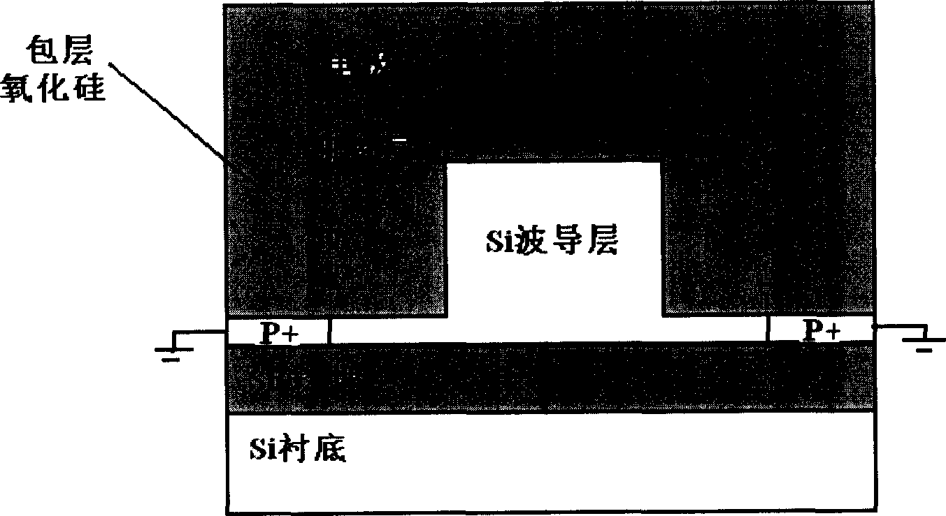
[0034] figure 1 Shown is a cross-sectional view of a common silicon-based MOS structure electro-optic modulator. The refractive index change region is within a limited range below the gate oxide layer in the silicon waveguide layer, and the large refractive index difference between the silicon oxide cladding layer and the core silicon waveguide layer confines the optical field in the silicon core layer.

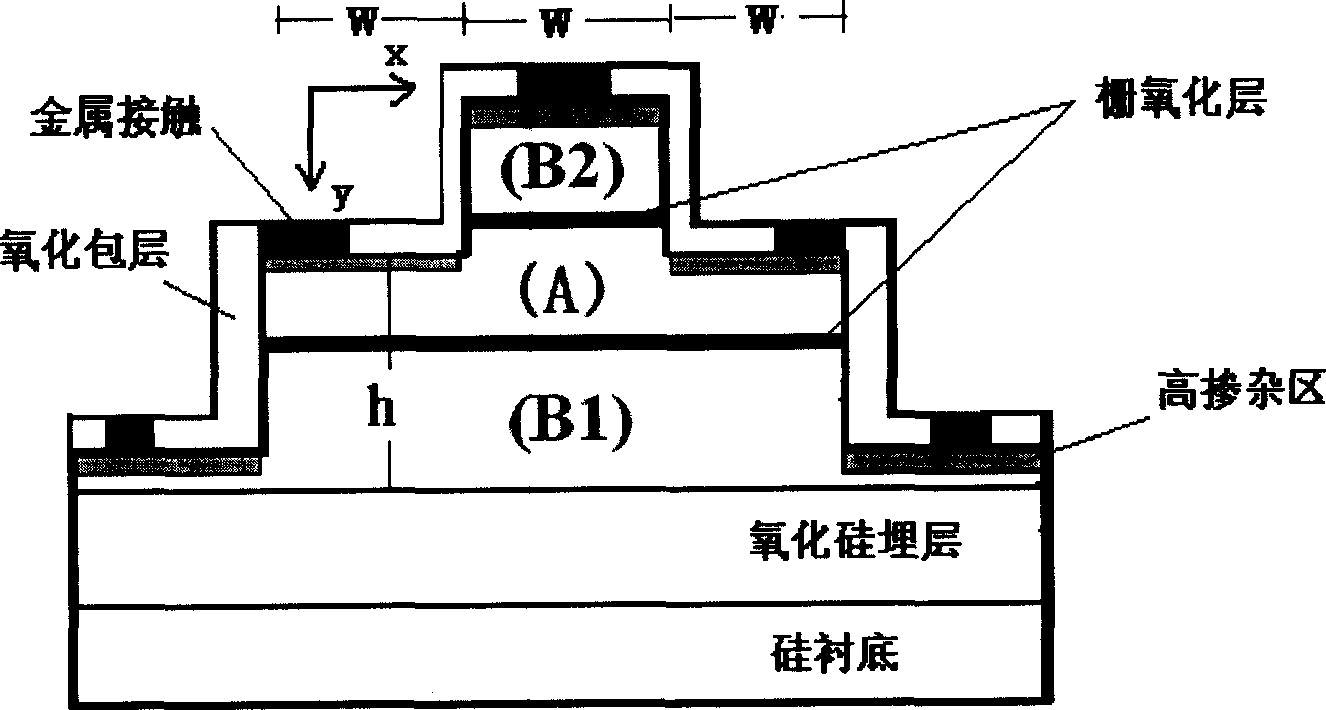
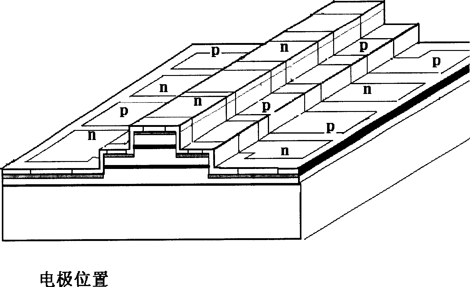
[0035] see figure 2 The schematic diagram of the cross-section of the electro-optic modulator with parallel MOS capacitor structure and image 3 Three-dimensional structure diagram of the device. Such as figure 2 , image 3 As shown, the structure includes SOI substrate, polysilicon-silicon dioxide symmetric structure (B1-A-B2) and cross-structure electrodes.

[0036] The polysilicon-silicon dioxide symmetric structure includes the core P-doped polysilicon, the inner cladding silicon oxide and the outer cladding N-doped polysilicon. Their thicknesses are: 1.3 μm, 10 n...


PUM

PropertyMeasurementUnit
Thicknessaaaaaaaaaa

Abstract

The related Si-base parallel MOS capacitor-structure high-speed electro-optical modulator comprises: the SOI substrate, some electrodes to form cross structure on modulation area surface, a dual-grid oxide layer clamped between the Si layers as n-p-n doping, a multi-crystal-Si waveguide layer, and a SiO2 layer, wherein the positive and negative electrodes form parallel capacitor structure as the source area, and it uses external voltage to control the range and quantity of free carrier concentration. This invention has high efficiency and compatible to traditional technology.

Description

technical field [0001] The invention relates to the technical field of photonics, in particular to a silicon-based parallel MOS capacitor structure high-speed electro-optic modulator and a manufacturing method. Background technique [0002] In recent years, with the continuous breakthrough of silicon-based materials in the field of photonics, people have to re-understand the development prospects of silicon materials in the field of optoelectronic integration. Silicon photonic devices are developing in the direction of small size, high speed and high stability. [0003] Current silicon optical modulators mainly include thermo-optic modulation, electro-optic modulation and optical-optic modulation. Thermo-optic modulators are stable, but device speeds tend to be low. Optical modulators are mostly in the research and development stage, and there is still a long way to go before practical applications. Electro-optic modulation is the most promising method to achieve large-sc...

Claims


Application Information

Patent Timeline
IPC IPC(8): G02F1/35
Inventor 屠晓光陈少武
Owner INST OF SEMICONDUCTORS - CHINESE ACAD OF SCI
Why Eureka
Try Eureka