Multiple field sheet type piezoresistor and its producing method

A varistor, multi-layer chip technology, applied in the direction of resistance manufacturing, varistor, varistor core, etc., can solve the problems of high cost of solder paste, poor solderability, unsuitable for mass production, etc.

Active Publication Date: 2007-02-07
SHENZHEN SUNLORD ELECTRONICS
View PDF0 Cites 17 Cited by
  • Summary
  • Abstract
  • Description
  • Claims
  • Application Information

AI Technical Summary

Problems solved by technology

At present, there is no structural standard for the surface material of chip varistors. A few multilayer chip varistors in the experimental stage use solderable solder paste to cover the surface of the terminal electrodes. They do not use tin plating, do not need electroplating, and the non-terminal electrode parts are also free of paste. Material surface treatment, this kind of experimental product has poor solderability when used, and the cost of solder paste is high, so it is not suitable for mass production

Method used


Image

  • Multiple field sheet type piezoresistor and its producing method
  • Multiple field sheet type piezoresistor and its producing method
  • Multiple field sheet type piezoresistor and its producing method

Examples


Embodiment 1

[0257] Embodiment 1: A multilayer chip varistor with an insulating layer between the internal electrodes and the terminal electrodes.

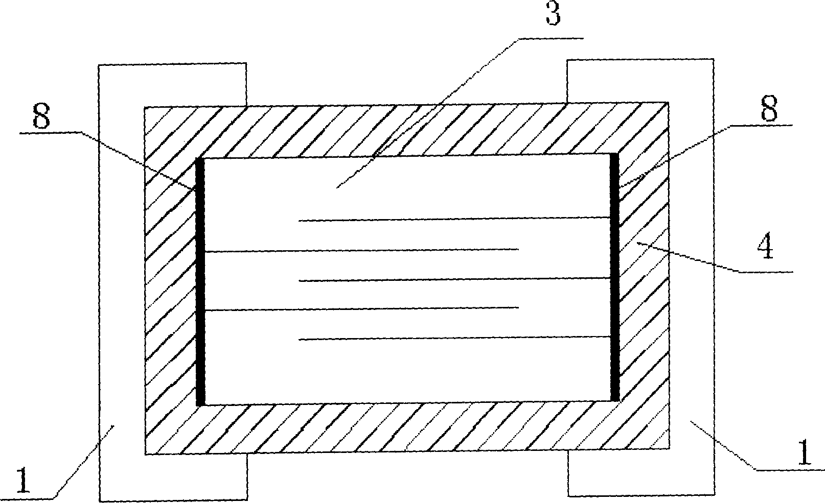
[0258] Such as image 3 The shown varistor with an insulating layer between the inner electrode and the terminal electrode is composed of a varistor substrate 3 , a terminal electrode 8 , a glass insulating layer 4 and a terminal electrode 1 .

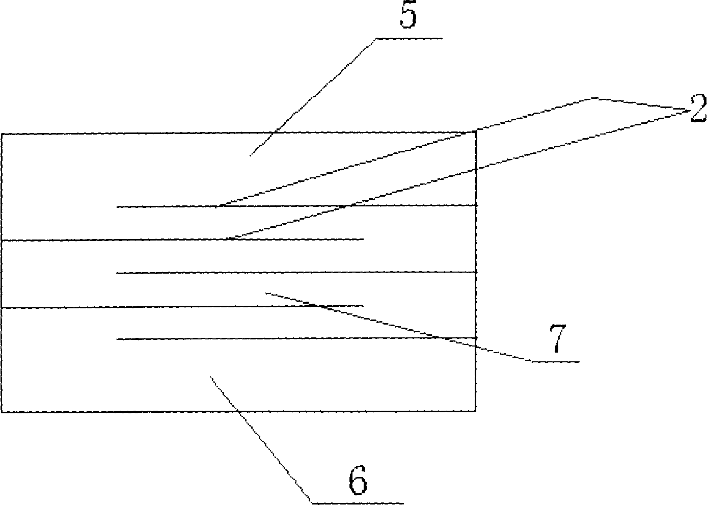
[0259] The two ends of the varistor substrate 3 are respectively provided with a terminal electrode 8 connected to a terminal electrode 1, and the internal electrode 2 at one end of each chip varistor unit is connected with the terminal electrode 8 at the corresponding end, The internal electrode 2 at the other end of each chip varistor unit is connected to the termination electrode 8 at the corresponding other end.

[0260] Its manufacture method comprises the following steps:

[0261] (1) Preparation of slurry

[0262] (1) The material components and weight percentages of the varistor film are res...

Embodiment 2

[0305] Embodiment 2: A multilayer chip varistor in which internal electrodes and terminal electrodes are directly connected.

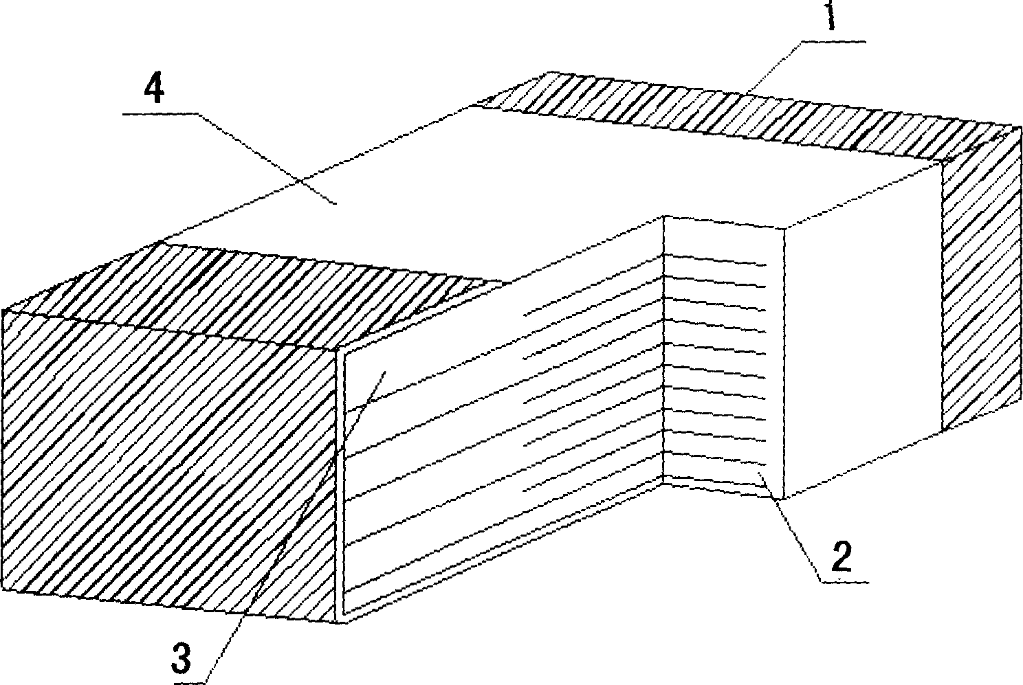
[0306] Such as Figure 4 The piezoresistor in which the inner electrode and the terminal electrode are directly connected is composed of a piezoresistor substrate 3 , a glass insulating layer 4 and a terminal electrode 1 .

[0307] The internal electrode at one end of each chip varistor unit is directly connected to the terminal electrode 1 at the corresponding one end, and the internal electrode at the other end of each chip varistor unit is directly connected to the terminal electrode 1 at the corresponding other end.

[0308] Its manufacture method comprises the following steps:

[0309] (1) prepare slurry, with embodiment 1 (one);

[0310] (2) lamination, with (two) of embodiment 1;

[0311] (3) cutting, with (3) of embodiment 1;

[0312] (4) degumming, with (four) of embodiment 1;

[0313] (5) sintering, with (five) of embodiment 1;

[0314]...

Embodiment 3

[0318] Embodiment 3: A multilayer chip varistor in which terminal electrodes are directly connected to a varistor substrate.

[0319] Such as Figure 5 The piezoresistor in which the terminal electrodes are directly connected to the piezoresistor substrate is composed of a piezoresistor substrate 3 , an organic material insulating layer 9 and a terminal electrode 1 .

[0320] The two ends of the varistor substrate are respectively directly connected to the two terminal electrodes 1;

[0321] The internal electrode at one end of each chip varistor unit is directly connected to the terminal electrode 1 at the corresponding one end, and the internal electrode at the other end of each chip varistor unit is directly connected to the terminal electrode 1 at the corresponding other end.

[0322] Its manufacture method comprises the following steps:

[0323] (1) Preparation of slurry

[0324] (1) The material of piezoresistive film is made into slurry, same as (1) (1) of embodiment...


PUM


Abstract

The invention relates to a multi-layer voltage-sensitive resistance and relative production, wherein it has the types as internal electrode and end electrode inside the insulated layer; the internal electrode and end electrode are connected directly; and the end electrode and the base board are directly connected; and the production comprises: preparing slurry, laminating layers, slicing, discharging adhesive, sintering, surface treating the insulated slurry of base board, producing two end electrodes and electrically plating. The invention insulated treats the surface of multi-layer sheet voltage-sensitive resistance without end electrodes, without water adsorption, and it plates nickel and tin on the surface of end electrode, to improve the welding property and the welding reliability, with lower cost and batch production.

Description

technical field [0001] The invention relates to a piezoresistor, in particular to a multilayer chip piezoresistor and a manufacturing method thereof. Background technique [0002] With the rapid development of electronic information systems, small chip varistors are widely used, which usually consist of a varistor substrate, internal electrodes inside the substrate, electrode paste on the surface of the substrate, glass materials or other materials. In the manufacturing process, the above-mentioned materials, structures and manufacturing processes all directly affect the performance of the product. At present, there is no structural standard for the surface material of chip varistors. A few multilayer chip varistors in the experimental stage use solderable solder paste to cover the surface of the terminal electrodes. They do not use tin plating, do not need electroplating, and have no paste on the non-terminal electrode parts. Material surface treatment, this kind of experi...

Claims


Application Information

Patent Timeline
Patent Type & Authority Applications(China)
IPC IPC(8): H01C7/10H01C7/108H01C17/00
Inventor 贾广平成学军施红阳李蕾郭海李有云
Owner SHENZHEN SUNLORD ELECTRONICS
Why Eureka
Try Eureka