Thin film transistor base plate

A technology of thin-film transistors and substrates, applied in the direction of electric solid-state devices, semiconductor devices, semiconductor/solid-state device components, etc., can solve problems such as limitations, affecting liquid crystal alignment, and brightness reduction

Active Publication Date: 2007-02-07
AU OPTRONICS CORP
View PDF0 Cites 12 Cited by
  • Summary
  • Abstract
  • Description
  • Claims
  • Application Information

AI Technical Summary

Problems solved by technology

[0004] In addition, when the black matrix (black matrix, BM) of the upper color filter substrate is combined with the lower thin-film transistor substrate, there will be a limit to the group accuracy, so the pixel design must take into account the process capability of the group accuracy. restricted
In addition, when the group dislocation occurs, it will reduce the aperture ratio and reduce the brightness, and even affect the alignment of the liquid crystal to cause disclination.

Method used


Image

  • Thin film transistor base plate
  • Thin film transistor base plate
  • Thin film transistor base plate

Examples


Embodiment 1

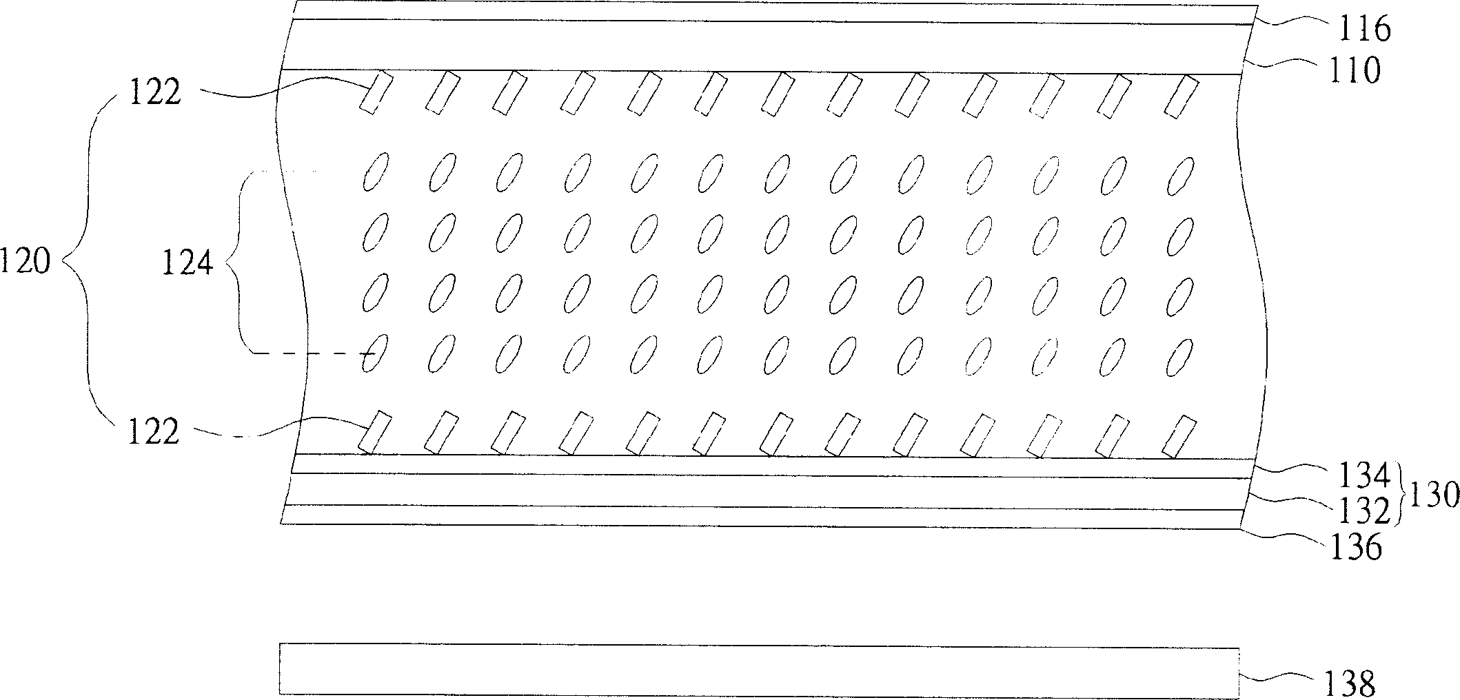
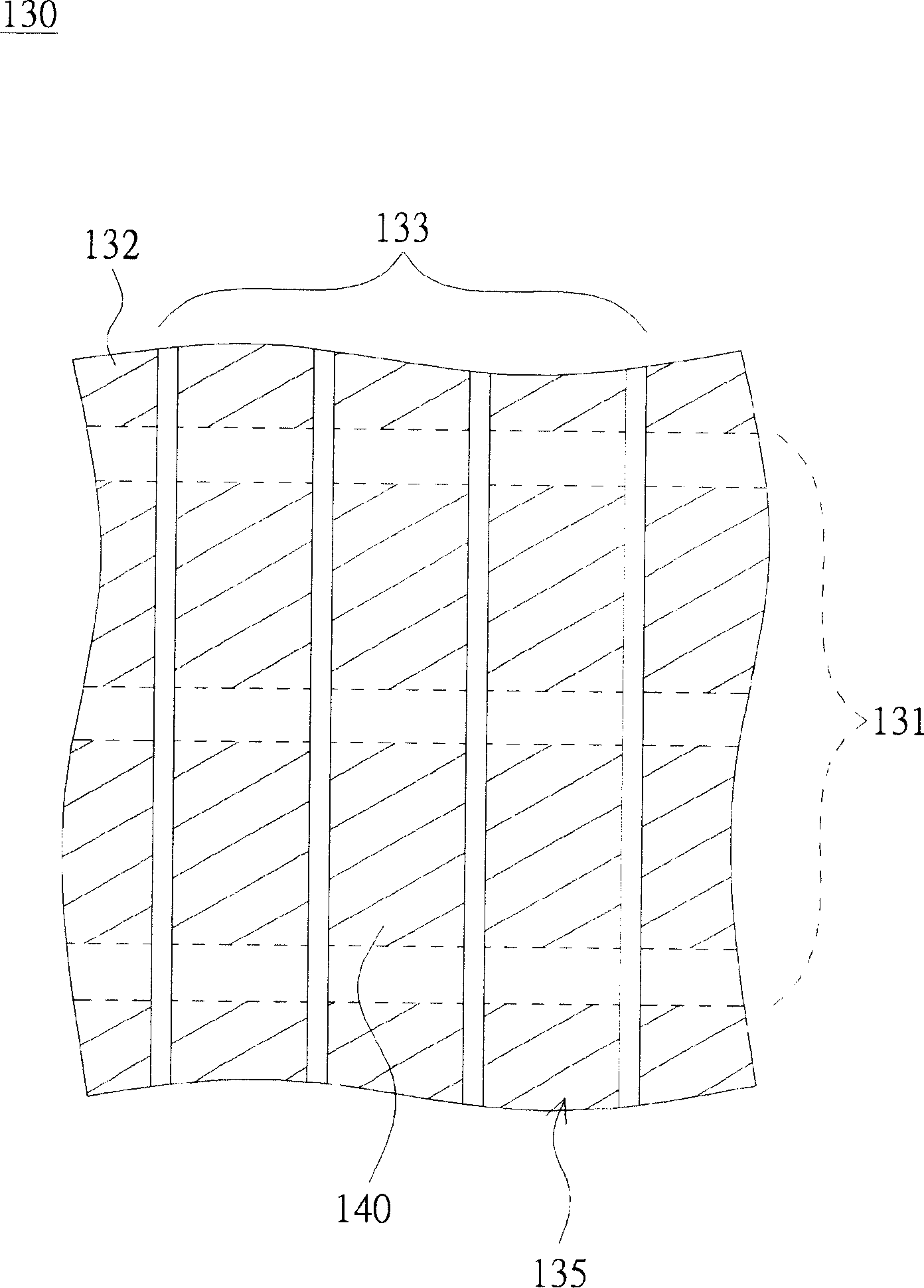
[0079] Please refer to Figure 3A , which is a partial schematic view showing the thin film transistor substrate of the first embodiment. The second substrate 130 includes a base 132 , a plurality of scan lines 131 , a plurality of data lines 133 and a pixel unit 140 . The scan lines 131 are disposed on the substrate 132 , the data lines 133 are disposed on the scan lines 131 , and the data lines 133 are perpendicular to the scan lines 131 to define a plurality of pixel regions 135 . The pixel unit 140 is disposed on the substrate 132 and located in the pixel area 135 therein. Please refer to Figure 3B , which is a schematic diagram showing the first pixel unit of the first embodiment. Figure 3A The scan lines 131 include a first scan line 131a and a second scan line 131b, Figure 3A The data lines 133 include a first data line 133a and a second data line 133b. The pixel unit 140 includes a thin film transistor 141 and a pixel electrode 142 . The thin film transistor 1...

Embodiment 2

[0089] Please refer to Figure 4A , which is a schematic diagram showing the first pixel unit of the second embodiment. The structures of the black matrix layer 220 and the color filter layer 230 are arranged on the thin film transistor substrate, such as Figure 4B shown. Please refer to Figure 4B , which is along Figure 4A The cross-sectional view taken by the section line AA'. the rest with Figure 3E and Figure 3C The same components continue to use the reference numerals and will not be described again. The protective layer 240 is disposed on the second insulating layer 146 and the pixel electrode 162 . The color filter layer 230 and the black matrix layer 220 are disposed on the protective layer 240 . In this embodiment, the pixel unit structure of the present invention is combined with a color filter on array (COA, color filter on array) process, and the black matrix layer 220 and the color filter layer 230 are disposed on the thin film transistor substrate. ...

Embodiment 3

[0093] Please refer to Figure 5A , which is a schematic diagram showing the first pixel unit of the third embodiment. In the pixel unit 310 of this embodiment, the structures of the black matrix 220 and the color filter layer 230 are arranged on the first substrate 110 (such as figure 2 shown) above. Also refer to Figure 5B , which is along Figure 5A The cross-sectional view taken by the section line AA'. the rest with Figure 3E and Figure 3C The same components continue to use the reference numerals and will not be described again. like Figure 5B As shown, the drain electrode 141b is electrically connected to the pixel electrode 312 through the second via hole 146b. The pixel electrode 312 is electrically connected to the second electrode 145 through the first through hole 146 a, so that the drain electrode 141 b has the same potential as the second electrode 145 . This structure can prevent the aperture ratio from being affected when there is an offset betwee...


PUM


Abstract

The invention relates to a film transistor base board, which comprises: substrate; several scanning wires; several data wires and pixel units, wherein the scanning wires are above the substrate; the data wires are above the scanning wires, while they are vertical to define several pixel areas; the pixel units are above the substrate and inside the pixel area; the pixel unit comprises film transistor and pixel electrode; the film transistor comprises source and drain; the pixel electrode is connected to the drain; the pixel electrode comprises the first bus electrode, the second bus electrode and several branched electrode; the first bus electrode is vertical to the second bus electrode; the branched electrode is connected to the first bus electrode and/or the second bus electrode; the first bus electrode uniformly divides the pixel area; and the film transistor is relative to one end of first bus electrode.

Description

technical field [0001] The invention relates to a thin film transistor substrate and a liquid crystal display device using the same, in particular to a thin film transistor substrate with a polymer auxiliary alignment layer and a liquid crystal display device using the same. Background technique [0002] In recent years, the technology of liquid crystal display (LCD) has advanced rapidly, and the key parameters of liquid crystal display devices, such as response time, viewing angle, brightness, contrast, etc., are actively seeking room for improvement. [0003] like figure 1 , which is a schematic diagram showing a thin film transistor substrate. In the pixel unit 10, in order to increase the aperture ratio, the through hole (through hole) connected to the thin film transistor 4 will be opened at the position of the common electrode 2, and the wire 1a of the second metal layer 1 (M2) will be used along the pixel electrode 3 The main line electrode 3a (main slit) is connect...

Claims


Application Information

Patent Timeline
Patent Type & Authority Applications(China)
IPC IPC(8): H01L27/12H01L23/522G02F1/136
Inventor 陈雅洁詹德威樊祥彬
Owner AU OPTRONICS CORP
Why Eureka
Try Eureka