

Motherboard of liquid crystal display and liquid crystal display faceplate
A liquid crystal display panel and liquid crystal display technology, which is applied to static indicators, instruments, etc., can solve the problems of scrapping liquid crystal display panels and reducing the yield of liquid crystal display panels.
- Summary
- Abstract
- Description
- Claims
- Application Information
AI Technical Summary
Problems solved by technology
Method used
Image

Examples
no. 1 example
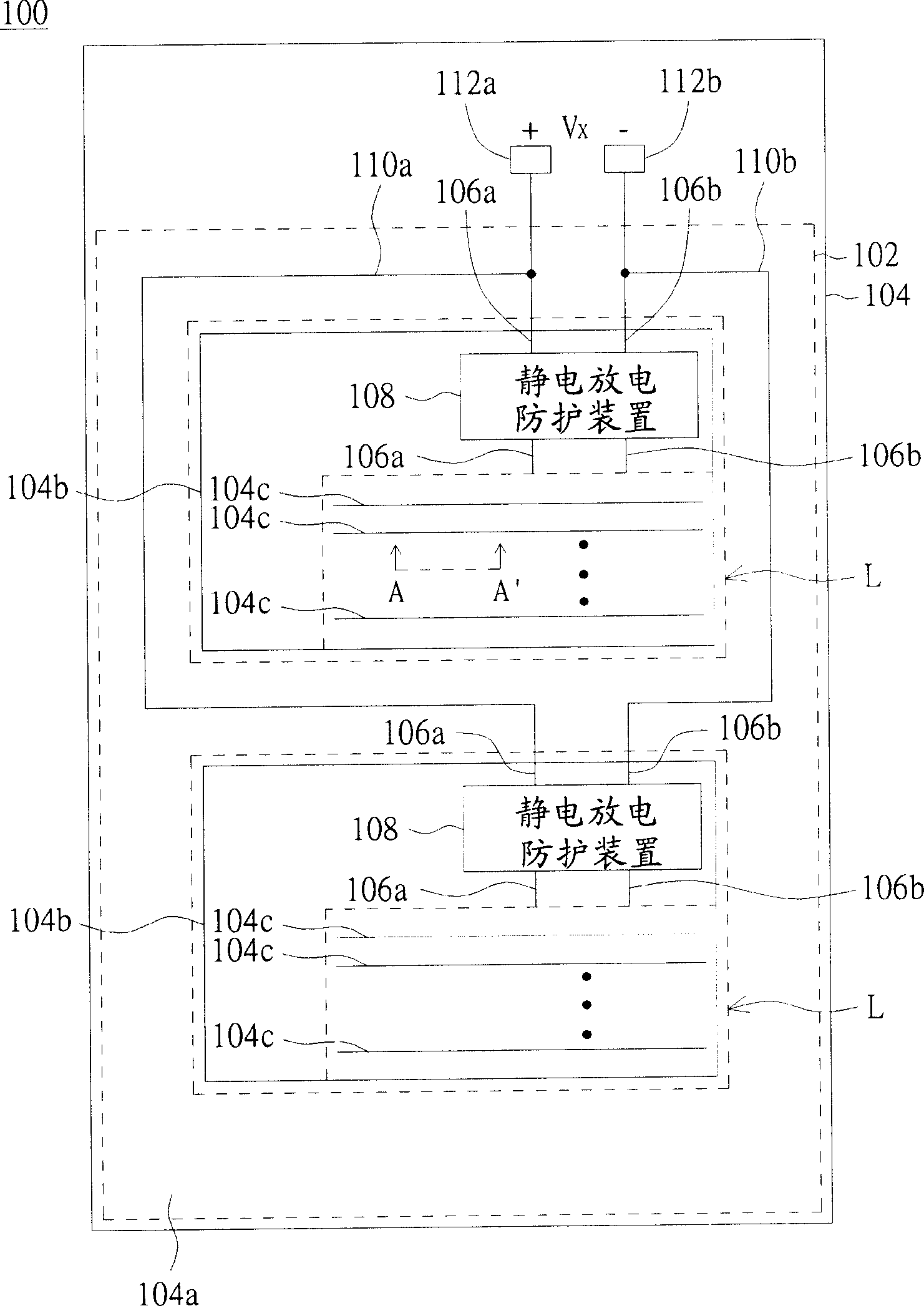
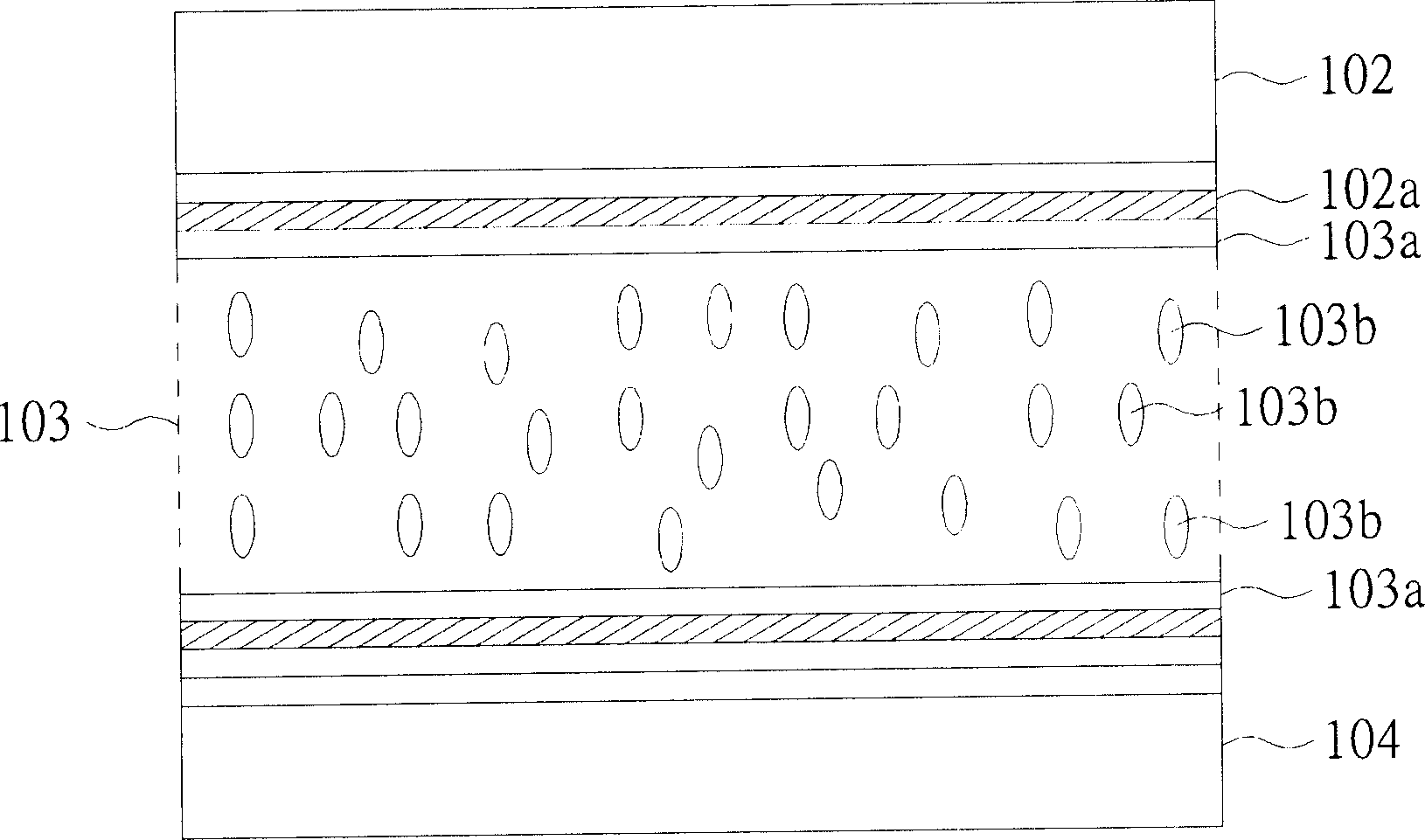
[0051] Please refer to Figure 1A and 1B , Figure 1A It shows the top structural view of the liquid crystal display motherboard of the first embodiment of the present invention, Figure 1B Shows Figure 1A The cross-sectional structure diagram of the cross-hatching line formed by A and A'. The liquid crystal display motherboard 100 includes a first substrate 102 , a second substrate 104 and a liquid crystal layer 103 . The second substrate 104 is disposed parallel to the first substrate 102 , and the second substrate 104 includes a non-panel area 104 a , a panel area 104 b , traces 106 a , 106 b , 110 a , 110 b and an ESD protection device 108 . Traces 106 a , 106 b and ESD protection device 108 are disposed on panel area 104 b , while traces 106 a and 106 b are electrically connected to ESD protection device 108 . Traces 110a and 110b are disposed on the non-panel region 104a and are electrically connected to traces 106a and 106b, respectively. Traces 110a and 110b are al...
no. 2 example
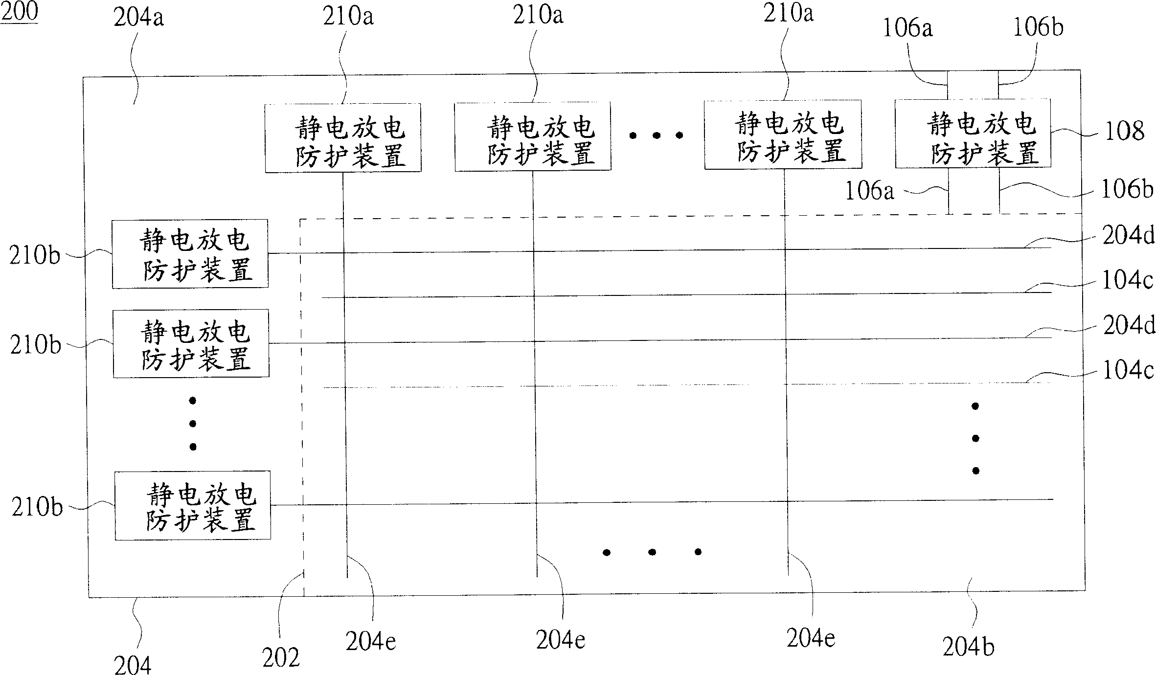
[0059] Please refer to Figure 4A and 4B , Figure 4A A circuit diagram showing the ESD protection device of the second embodiment of the present invention, Figure 4B Shows Figure 4A The cross-sectional structure diagram of the cross-hatching line formed by A and A'. The difference between this embodiment and the first embodiment is that this embodiment makes the wiring 406a, 406b, 410a and 410b a double metal wiring structure, and the wiring 406a and 410a and the wiring 406a The boundaries with 410b are respectively connected by traces 402a and 402b of a single metal layer (Single Metal) structure. There is an insulating layer 404a between the double metal layers of the traces 406a and 410a, and a contact hole (Contact Hole) 404b is formed in the insulating layer 404a, so that the double metal layers of the traces 406a and 410a can be electrically connected through the contact hole 404b. Next, the situation that the electrostatic discharge current generated by the elec...
no. 3 example
[0063] Please refer to Figure 5 , which shows another circuit diagram of the ESD protection device according to the third embodiment of the present invention. The difference between this embodiment and the first embodiment is that this embodiment uses a lightning rod (Lightning Protector) 502 to electrically connect to the traces 506a and 506b respectively, and the circuit structure of the lightning rod 502 and the traces 506a and 506b is used as ESD protection device 508 . In this way, when the electrostatic discharge generates an electrostatic discharge current, the lightning rod 502 can discharge the electrostatic discharge current through the tip discharge mechanism, preventing the electrostatic discharge current from being introduced into the liquid crystal display panel to achieve the electrostatic discharge protection effect.
PUM
 Abstract
Description
Claims
Application Information