Plasma display panel and its manufacture method

A technology for a display panel and a manufacturing method, applied in the direction of alternating current plasma display panels, cold cathode manufacturing, electrode system manufacturing, etc., capable of solving the problems of deterioration of discharge characteristics and high driving voltage of plasma display panels, and achieving lower discharge voltage and stable discharge characteristics Effect

Inactive Publication Date: 2007-02-21
LG ELECTRONICS(NANJING) PLASMA CO LTD
View PDF0 Cites 0 Cited by
  • Summary
  • Abstract
  • Description
  • Claims
  • Application Information

AI Technical Summary

Problems solved by technology

In addition, the discharge characteristics of the plasma display panel will also deteriorate, requiring a high driving voltage

Method used


Image

  • Plasma display panel and its manufacture method
  • Plasma display panel and its manufacture method
  • Plasma display panel and its manufacture method

Examples


Embodiment Construction

[0042] Hereinafter, preferred embodiments are given, and detailed descriptions are given in conjunction with the accompanying drawings.

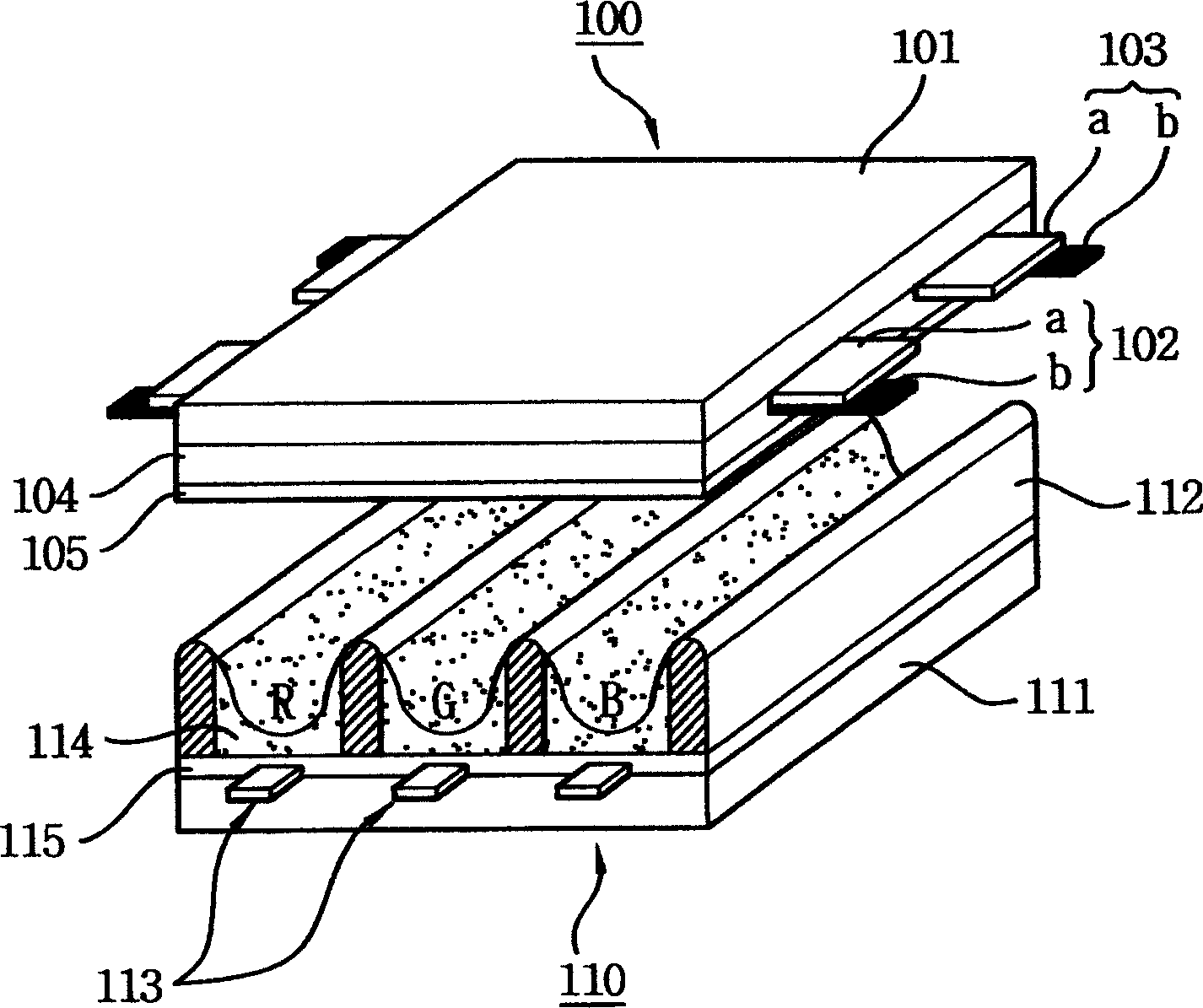
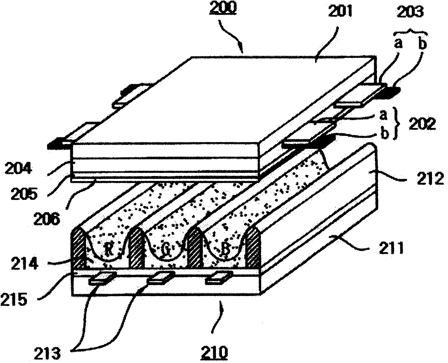
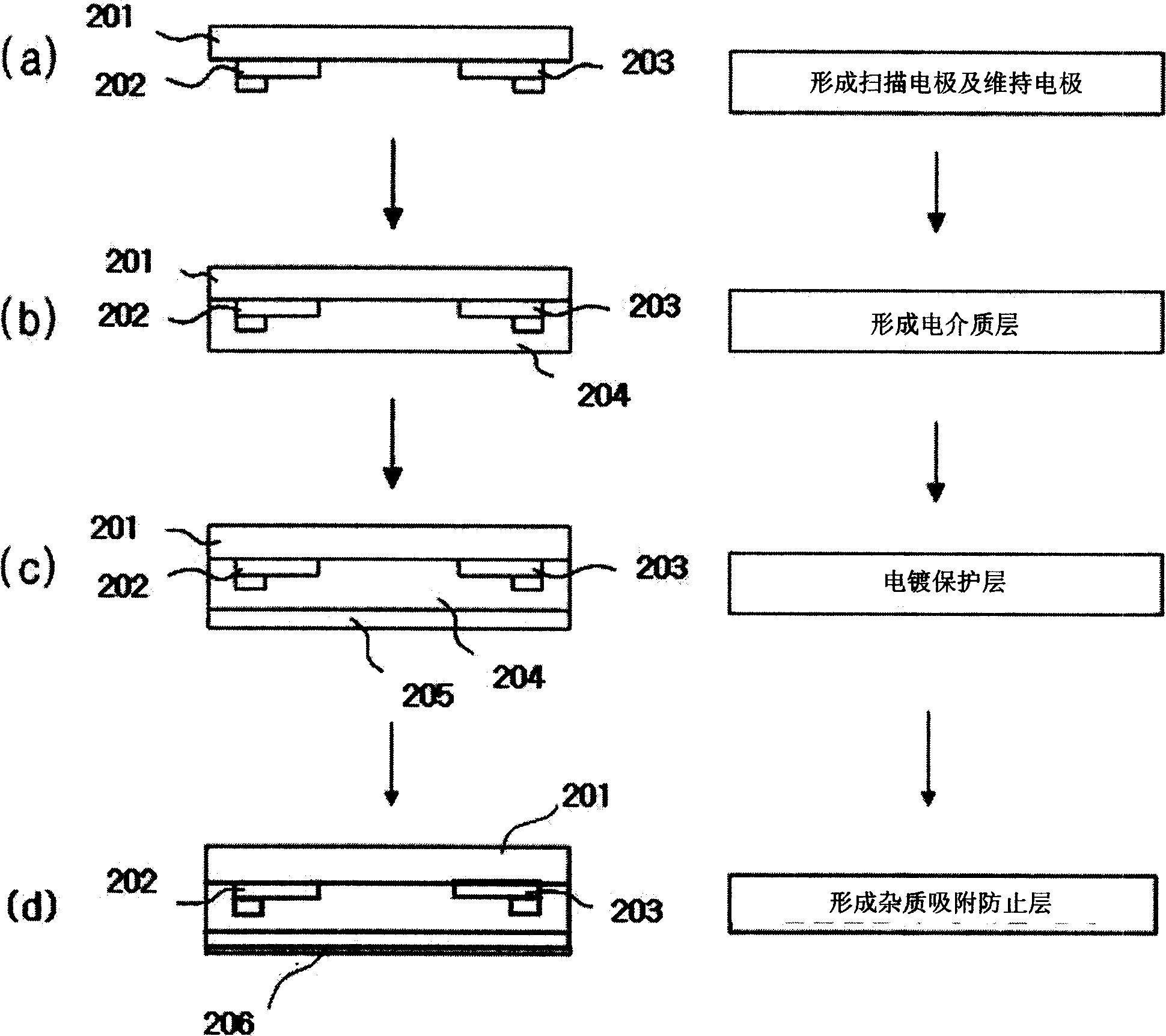
[0043] figure 2 It is a schematic diagram of the structure of the plasma display panel in the first embodiment of the present invention. Such as figure 2 As shown, the plasma display panel in the first embodiment of the present invention is composed of a front substrate 200 and a rear substrate 210 .

[0044] The front substrate 200 discharges each other in a discharge cell (cell), and the sustain electrode 202 and the scan electrode 203 that sustain the cell (cell) emit light, that is, the transparent electrode (a) and the transparent electrode (a) formed of a transparent ITO (Indium Thin Oxide) material. Sustain electrodes 202 and scan electrodes 203 composed of bus electrodes (b) made of metal materials are covered with one or more dielectric layers 104 that limit discharge current and insulate electrode pairs. On the dielectric laye...


PUM


Abstract

The present invention discloses a plasma display panel and the manufacture method thereof. The manufacture method of the plasma display panel of the present invention comprises a step of forming a protection layer on the substrate; a step of forming an impurity adsorption preventing layer to prevent the surface of the protection layer from adsorbing impurity. The plasma display panel of the present invention comprises a protection layer formed on the substrate; and an impurity adsorption preventing layer formed on the surface of the protection layer. The present invention is capable of forming an impurity adsorption preventing layer on the protection layer, so that the protection layer is prevent from adsorbing water(H2O)or carbon dioxide(CO2), etc,. Wherein the plasma display panel has stable discharging characteristic and is capable of effectively emitting secondary electron and reducing the discharge voltage.

Description

1. Technical field [0001] The present invention relates to a plasma display panel, more specifically, a plasma display panel with stable discharge characteristics and capable of effectively emitting secondary electrons and a manufacturing method thereof. 2. Background technology [0002] A general plasma display panel (Plasma Display Panel) consists of a spacer formed between the upper substrate and the lower substrate to form a unit cell (cell), and each cell (cell) is filled with neon (Ne), helium (He), Or the main discharge gas such as the mixed gas of neon and helium (Ne+He) and a small amount of inert gas containing xenon. When the high-frequency voltage causes discharge, the inert gas generates vacuum ultraviolet rays (Vacuum Ultraviolet ray), which makes the phosphors formed between the interlayers emit light and display images. Such a plasma display panel has a light and thin structure, and is attracting attention as a next-generation display device. [0003] figu...

Claims


Application Information

Patent Timeline
Patent Type & Authority Applications(China)
IPC IPC(8): H01J9/00C25D3/00H01J17/02H01J17/49H01J11/40
CPCH01J9/02H01J9/241H01J11/12H01J11/40
Inventor 李范周崔伦永李暻和郑宰祥
Owner LG ELECTRONICS(NANJING) PLASMA CO LTD
Why Eureka
Try Eureka