Dynamically biased amplifier

A technology of amplifiers and operational amplifiers, applied in the fields of amplifiers, improving amplifiers to increase efficiency, and components of amplifying devices, etc., can solve the impossible, the bias circuit is not suitable for the use of high-frequency RF signals, and the difficulty of creating bias adjustment signals and other problems, to achieve the effect of linear increase and reduction of intermodulation distortion

Active Publication Date: 2007-02-21
TELEFON AB LM ERICSSON (PUBL)
View PDF1 Cites 9 Cited by
  • Summary
  • Abstract
  • Description
  • Claims
  • Application Information

AI Technical Summary

Problems solved by technology

In particular, it is extremely difficult and close to impossible to detect RF signals with frequencies around 100MHz or GHz and create a bias adjustment signal fr

Method used


Image

  • Dynamically biased amplifier
  • Dynamically biased amplifier
  • Dynamically biased amplifier

Examples


Embodiment Construction

[0046] Throughout the drawings, the same reference numerals will be used for corresponding or similar elements.

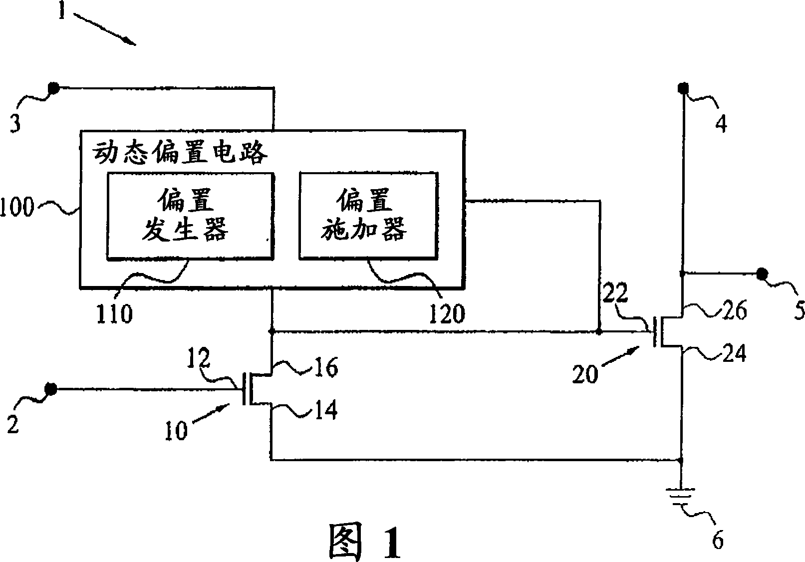
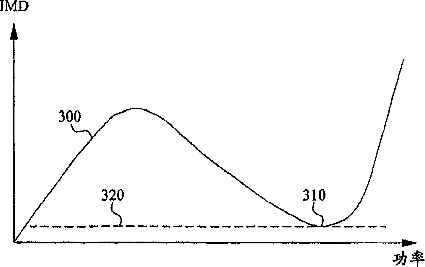
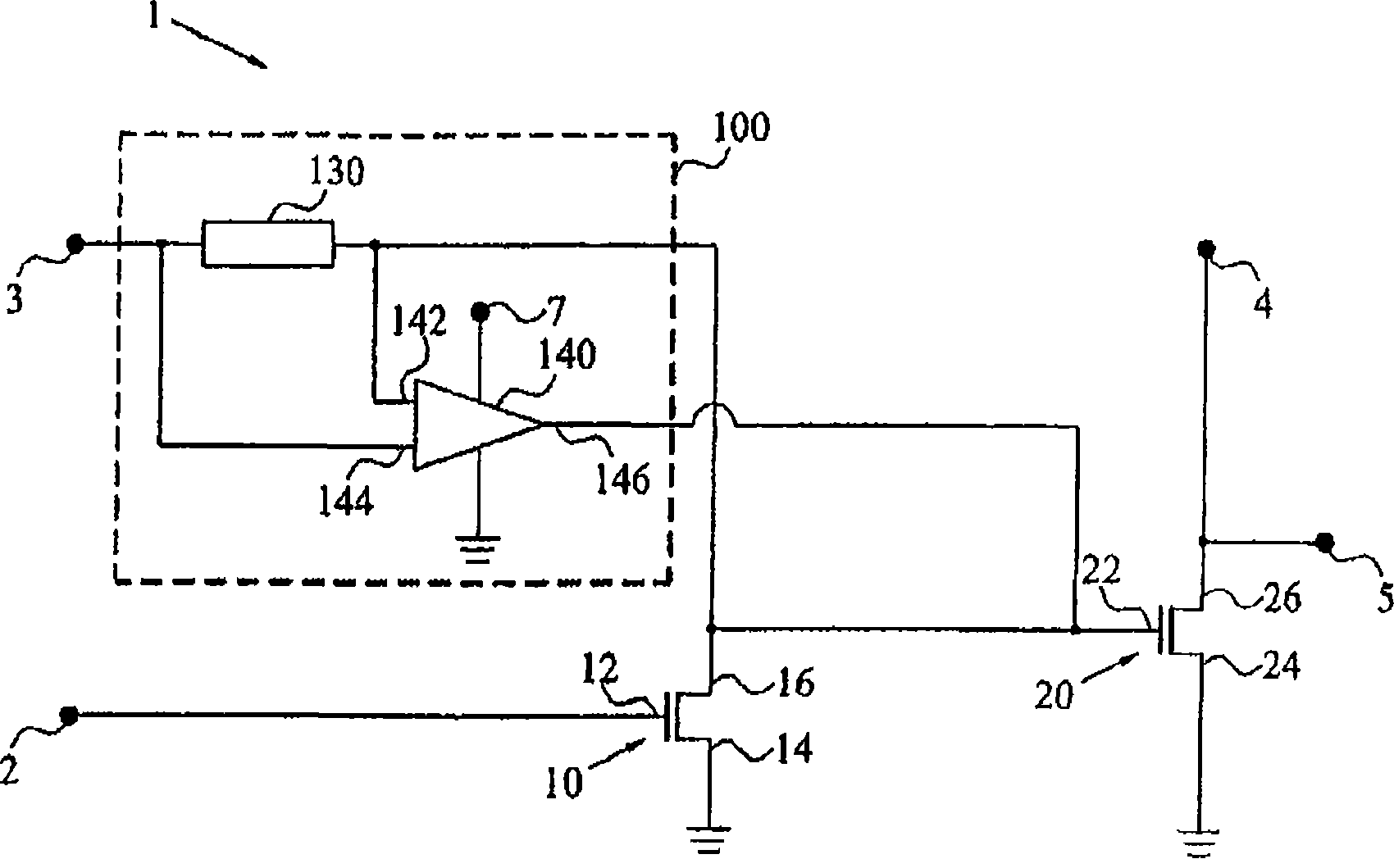
[0047] The present invention relates to dynamic biasing of transistors in amplifiers in order to reduce or suppress intermodulation distortion (IMD) and increase amplifier linearity.

[0048]In general, for a given output or input power level of the amplifier, a bias signal can be adjusted and applied in order to improve the IMD, ie reduce the IMD. Since output and input power are time-dependent, the bias signal should follow this power change. The present invention provides a dynamic bias circuit for use in an amplifier that is capable of generating a bias signal based on the input (and output) power level of the amplifier.

[0049] The dynamic biasing circuits and amplifiers described and disclosed herein are particularly useful in wireless communication applications. However, other applications are readily known to those skilled in the art.

[0050] Figure 1 ...


PUM


Abstract

The present invention provides dynamic biasing of transistor in an amplifier comprising at least two interconnected transistor provided for processing an input signal. Once the input signal is applied to a driver transistor, a DC current signal of the output electrode of this transistor is detected. This DC current detection could be implemented as a detection of a voltage drop by providing the DC current signal to a resistor. A dynamic bias signal is then generated based on this detected DC current signal or voltage drop proportional to the DC current signal. The bias signal is applied to an input electrode of a final transistor for providing dynamic biasing thereof. The biasing of the invention reduces the intermodulation distortion of the final transistor and amplifier. In addition, the biasing enables an automatic change of operation class for the transistor.

Description

technical field [0001] The present invention relates generally to amplifiers and amplifier stages, and in particular to dynamic biasing of such amplifiers and amplifier stages. Background technique [0002] Radio frequency (RF) power amplifiers, such as transmitters in wireless communication systems, typically include interconnected transistor circuits for amplifying RF signals to high power levels. The amplified RF signal can then be transmitted into space via the antenna. [0003] Modern wireless communication systems rely on complex digital modulation schemes and the use of multiple carriers to meet the requirement of high data transmission capacity over a minimum frequency spectrum. Consequently, amplified RF signals to be transmitted and received typically have complex and strongly time-varying envelopes. This composite signal behavior can produce different forms of distortion, including adjacent and alternating channel distortion and intermodulation distortion (IMD)....

Claims


Application Information

Patent Timeline
IPC IPC(8): H03F1/02H03F1/30
CPCH03F1/301H03F1/0266H03F2200/18
Inventor H·韦佐维克
Owner TELEFON AB LM ERICSSON (PUBL)
Why Eureka
Try Eureka