
Method for determining lens errors in a particle-optical device

A particle optics and lens technology, which is applied in the field of determining the lens error in particle optics equipment, and can solve problems such as the lack of a clear image of the solder ball and the difficulty in determining the lens error.

Active Publication Date: 2007-03-07
FEI CO
View PDF0 Cites 7 Cited by
  • Summary
  • Abstract
  • Description
  • Claims
  • Application Information

AI Technical Summary

Problems solved by technology

So there is no clear image of the solder ball in any direction, which makes it difficult to determine the lens error

Method used


Image

  • Method for determining lens errors in a particle-optical device
  • Method for determining lens errors in a particle-optical device

Examples


Embodiment Construction

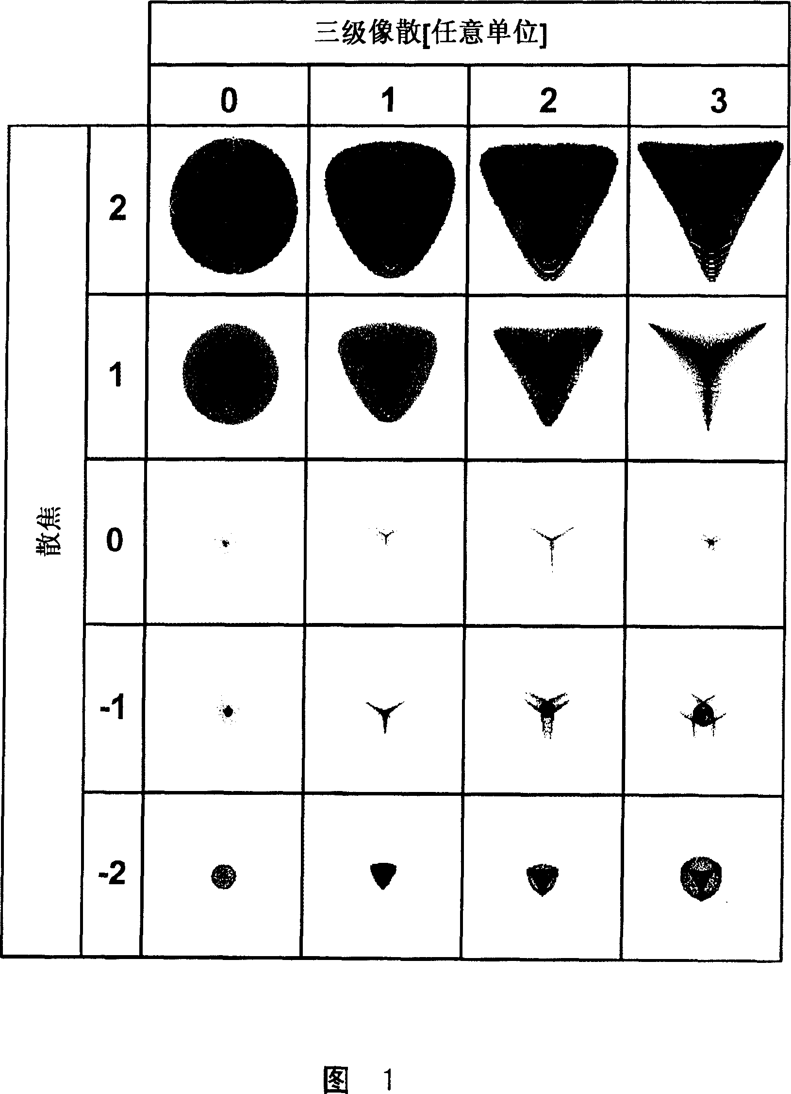
[0049] Figure 1 shows diagrammatically the cross-sections of the beam at different distances from the (paraxial) focal plane calculated by computer simulation.

[0050] In this simulation, the beams were subjected to the same degree of spherical aberration in all cases. Rows show cross-sections at different degrees of defocus, while columns show cross-sections at different values ​​of tertiary astigmatism.

[0051] The focal plane is shown in the third row at "Defocus=0". The second row shows the cross-section of the beam in a plane that is placed some distance behind the focal plane as seen from the objective, while the first row shows the same distance behind the focal plane The cross section of the beam in the plane at . Similarly, the fourth and fifth rows show the cross-section of the beam in the plane between the paraxial focal plane and the objective.

[0052] Far to the left of the first column, there is no third-order astigmatism, and the beam experiences only sphe...


PUM

PropertyMeasurementUnit
Biggest sizeaaaaaaaaaa

Abstract

The invention relates to a method for determining lens errors in a Scanning Electron Microscope, more specifically to a sample that enables such lens errors to be determined. The invention describes, for example, the use of cubic MgO crystals which are relatively easy to produce as so-called 'self-assembling' crystals on a silicon wafer. Such crystals have almost ideal angles and edges. Even in the presence of lens errors this may give a clear impression of the situation if no lens errors are present. This enables a good reconstruction to be made of the cross-section of the beam in different under- and over-focus planes. The lens errors can then be determined on the basis of this reconstruction, whereupon they can be corrected by means of a corrector.

Description

technical field [0001] The present invention relates to a method for determining lens error in a particle optics device designed to scan a sample with a focused particle beam, comprising: [0002] provide a sample containing parts of known shape, [0003] generating one or more images of the sample by scanning the sample with a particle beam, and [0004] The cross-section of the beam is determined based on the generated image. Background technique [0005] One such method is disclosed in the catalogue "Scanning Electron Microscopy Supplies" from Canemco, (821B McCaffrey St., St. Laurent, (Montreal) Quebec, Canada H4T 1N3), p. 29 ("Low Voltag Resolution Tinon Carbon"). For example, this can be read from the Internet on August 25, 2005 ( http: / / www.canemco.com / catalog / sem / Canemco Scanning.pdf ) is obtained. [0006] The method is used in conjunction with particle optics equipment such as SEM (Scanning Electron Microscope), STEM (Scanning Transmission Electron Microscope...

Claims


Application Information

Patent Timeline
IPC IPC(8): G01N13/10H01J37/26G01B15/00
CPCH01J37/28H01J2237/282H01J37/153
Inventor D·J·马斯S·A·M·门廷克J·J·L·霍里克希B·H·弗雷塔格
Owner FEI CO
Learn More