Thin packing structure for enhancing crystal fin radiation

A thin, crystal-backed technology, applied in semiconductor/solid-state device manufacturing, semiconductor/solid-state device components, semiconductor devices, etc., can solve the problems of inability to improve heat dissipation efficiency and inconvenience, prevent overflow glue from flowing in, and enhance chip structural strength , Improve the effect of heat dissipation

Inactive Publication Date: 2007-04-04
CHIPMOS TECH INC
View PDF1 Cites 8 Cited by
  • Summary
  • Abstract
  • Description
  • Claims
  • Application Information

AI Technical Summary

Problems solved by technology

A sealant 30 is to seal the active surface 11 of the chip 10 and the upper surface 22 of the substrate 20, but the back side 12 of the chip 10 is directly exposed to the lower surface 23 of the substrate 20, so that the heat generated by the chip 10 during operation , through the back side 12 to directly dissipate heat, but the known heat dissipation efficiency of the chip 10 is related to the exposed surface area of ​​the chip back side 12, and the maximum surface area exposed on the chip back side in the existing conventional packaging structure is only the size of the chip, It cannot be increased, so the maximum heat

Method used


Image

  • Thin packing structure for enhancing crystal fin radiation
  • Thin packing structure for enhancing crystal fin radiation
  • Thin packing structure for enhancing crystal fin radiation

Examples


no. 1 Embodiment

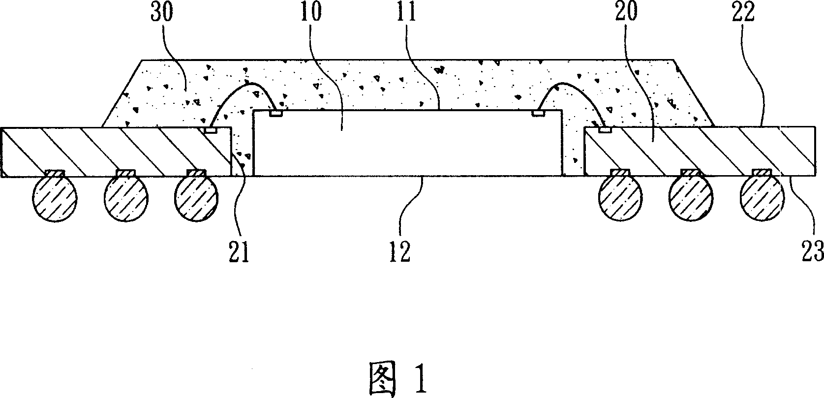
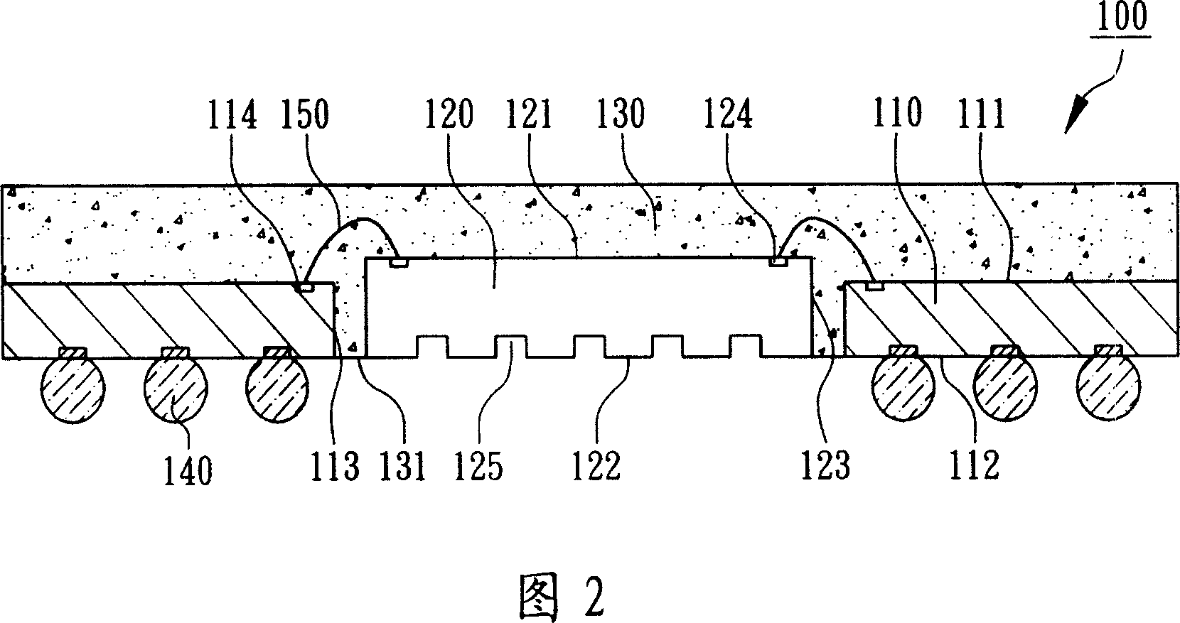
[0070] Please refer to FIG. 2 , which is a schematic cross-sectional view of a thin package structure for improving heat dissipation on the crystal back according to the first embodiment of the present invention. The thin package structure 100 for improving heat dissipation on the crystal back is in the form of a Ball Grid Array (BGA) package. The thin packaging structure 100 mainly includes a substrate 110, a chip 120 and a sealing compound 130, wherein:

[0071] The substrate 110 has an upper surface 111 , a lower surface 112 and a capacitive hole 113 passing through the upper surface 111 and the lower surface 112 . During the packaging process, the substrate 110 is not used to directly carry the chip 120 , but is attached to the lower surface 112 of the substrate 110 with a temporary adhesive tape (not shown) to bond and fix the chip 120 . Therefore, the chip 120 can be accommodated in the crystal hole 113 of the substrate 110;

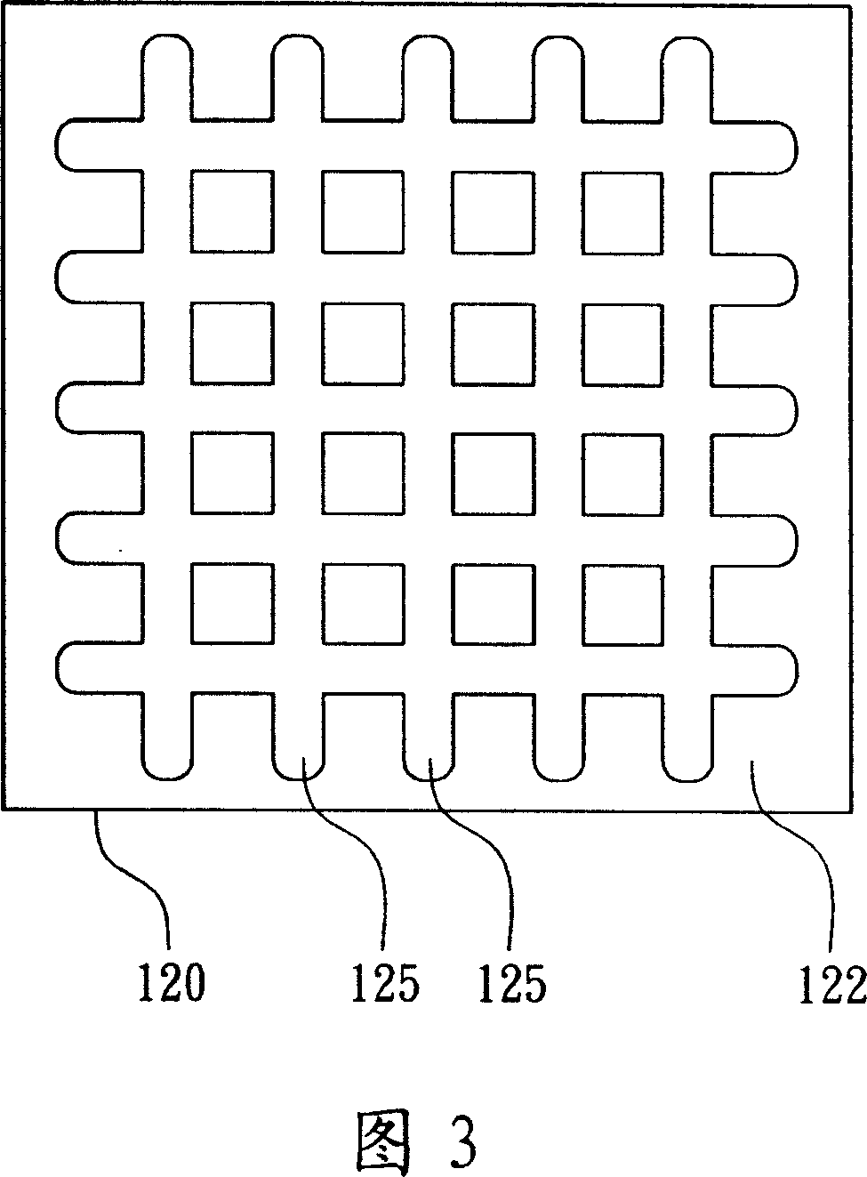
[0072] The wafer 120 has an active surface...


PUM


Abstract

The invention is concerned with the thin sealing structure for enhancing the radiation of the wafer back, including: the base panel, the wafer, and the sealing colloid; the base panel is with the upper surface, the under surface, and the transfixing geode; the wafer is contained at the geode of the base panel and with the initiative surface and the back surface, the initiative surface forms plural number of welding underlay and electric connects with the base panel, the back surface of the wafer forms plural number of the grooves; the sealing colloid forms on the upper surface of the base panel, covers the initiative surface of the wafer, and show the back surface and the grooves of the wafer, therefore the grooves is with the effects to enhance the radiation of the wafer back and intensity of the wafer.

Description

technical field [0001] The invention relates to an integrated circuit package structure with an exposed crystal back, in particular to a thin package structure which improves heat dissipation of the crystal back. Background technique [0002] As the packaging technology of integrated circuits becomes lighter, thinner, shorter, and smaller, the demand for heat dissipation is getting higher and higher. Generally, a heat sink is added to the packaging structure to improve the heat dissipation of the packaging structure, but it will increase the heat dissipation of the packaging structure. Therefore, considering the total thickness of the package, a package structure that directly exposes the back of the chip to improve heat dissipation has been developed. As disclosed in US Pat. No. 5,696,666, please refer to FIG. 1, which is a schematic cross-sectional view of a conventional ball grid array package structure with an exposed crystal back. The conventional integrated circuit pac...

Claims


Application Information

Patent Timeline
IPC IPC(8): H01L23/367H01L23/28H01L21/56
CPCH01L2924/18165H01L2924/15311H01L2924/10158H01L2924/15151H01L2224/48227H01L2924/181H01L2224/48091H01L2924/00012H01L2924/00014
Inventor 吴政庭邱士峰潘玉堂陈廷源张育诚苏铭弘
Owner CHIPMOS TECH INC
Why Eureka
Try Eureka